Design Rule Checking (DRC) in VLSI Physical Verification


1. Introduction to Physical Verification in VLSI Design
Physical verification is a critical step in the VLSI design flow, ensuring that the integrated circuit (IC) layout adheres to the manufacturing constraints defined by the foundry.
Among the various checks performed, Design Rule Checking (DRC) is a cornerstone of physical verification, validating that the layout complies with geometric and connectivity rules to ensure manufacturability, reliability, and high yield.
1.1. Importance of DRC
- Manufacturability: Ensures the layout can be fabricated without defects like shorts, opens, or misalignments.
- Yield Optimization: Compliance with design rules maximizes the percentage of functional chips.
- Reliability: Prevents issues like electromigration or time-dependent dielectric breakdown.
- Signoff Requirement: Foundry acceptance for tape-out requires a DRC-clean layout.
1.2. Context in the VLSI Design Flow
- DRC is performed post-placement and routing, during the physical design signoff phase.
- It is part of a broader physical verification suite, including Layout vs. Schematic (LVS), Electrical Rule Checking (ERC), and Antenna checks.
- DRC violations must be resolved before tape-out to avoid costly re-spins.
2. Fundamentals of Design Rule Checking
2.1. What is DRC?
DRC is an automated process that verifies whether the IC layout satisfies the geometric and connectivity constraints specified in the foundry's Process Design Kit (PDK). These constraints, or design rules, account for the limitations of semiconductor manufacturing processes, such as lithography, etching, and deposition.

2.2. Why DRC is Necessary
- Process Imperfections: Manufacturing equipment has inherent tolerances (e.g., overlay errors, critical dimension variations).
- Physical Limitations: Minimum feature sizes are constrained by lithography resolution and material properties.
- Yield and Reliability: Violations can lead to defects (e.g., shorts, opens) or performance degradation.
- Foundry Requirements: Non-compliant layouts are rejected to avoid fabrication risks.
2.3. DRC in the PDK
- The PDK contains the DRC rule deck, a set of scripts defining geometric constraints for each process layer.
- Rules are provided by foundry process engineers and tailored to specific process nodes (e.g., 7nm, 5nm).
- Examples include minimum wire width, spacing, enclosure, and density requirements.
3. Common Types of DRC Rules
DRC rules vary by process node and foundry but can be categorized into several core types. Below is an expanded list with detailed explanations:
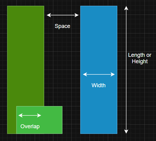
3.1. Minimum Width Rules
- Definition: Specifies the minimum allowable width for features (e.g., metal wires, polysilicon gates).
- Purpose: Ensures features are robust against process variations and electromigration.
- Example: A metal 1 (M1) layer may require a minimum width of 40nm to ensure reliable patterning.
- Violation Impact: Narrow features may fail to print or suffer from high resistance.
3.2. Minimum Spacing Rules
- Definition: Defines the minimum distance between adjacent features on the same or different layers.
- Purpose: Prevents short circuits and reduces parasitic capacitance.
- Special Cases:
- End-of-Line (EOL) Spacing: Additional spacing at line ends to account for lithographic widening.
- Different-Net Spacing: Larger spacing between features on different nets to avoid crosstalk.
- Example: Two M1 wires must be at least 50nm apart to prevent shorts.
3.3. Enclosure (Overlap) Rules
- Definition: Requires one layer to fully enclose another by a specified margin.
- Purpose: Ensures reliable connections and prevents open circuits.
- Example: A via must be enclosed by M1 and M2 layers by at least 10nm to ensure proper contact.
- Violation Impact: Inadequate enclosure may lead to incomplete vias or misalignment.
3.4. Minimum Area Rules
- Definition: Specifies the minimum area for a polygon on a given layer.
- Purpose: Prevents features from being too small to fabricate reliably.
- Example: A diffusion region must have a minimum area of 0.1µm² to ensure proper patterning.
- Related Rules: Minimum hole area rules prevent small voids in large polygons.
3.5. Notch and Slot Rules
- Definition: Regulates narrow gaps (notches) or slots within polygons.
- Purpose: Prevents manufacturing issues like incomplete filling or parasitic effects.
- Example: A notch in a metal layer must be at least 30nm wide to avoid patterning defects.
3.6. Density Rules
- Definition: Ensures uniform feature density across the chip to facilitate chemical-mechanical polishing (CMP).
- Purpose: Prevents dishing or erosion during CMP.
- Example: Metal layer density must be between 20% and 80% within a specified window.
- Fix: Dummy fill patterns are added to meet density requirements.
3.7. Advanced Rules
- Antenna Rules: Limit the ratio of metal area to gate area to prevent plasma-induced damage during fabrication.
- Double Patterning Rules: Assign features to different masks for sub-14nm nodes to overcome lithographic limits.
- Via Stacking Rules: Restrict the number of vertically stacked vias to ensure reliability.
- Wide Metal Rules: Require slots or spacing for wide metal lines to prevent stress-induced defects.
4. DRC in Advanced Process Nodes
As process nodes shrink (e.g., 7nm, 5nm, 3nm), DRC becomes increasingly complex due to:
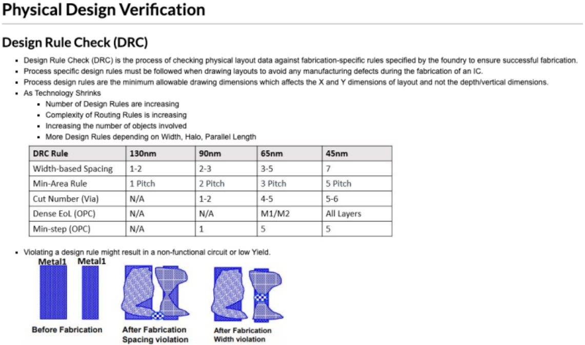
4.1. Tighter Geometries
- Smaller feature sizes demand stricter rules (e.g., 20nm minimum pitch in 5nm nodes).
- Increased sensitivity to process variations requires larger margins.
4.2. Multi-Patterning Technologies
- Double/Triple Patterning: Features are split across multiple masks, introducing new rules for mask assignment and alignment.
- Extreme Ultraviolet (EUV) Lithography: While EUV simplifies some patterning, it introduces unique rules for stochastic defects.
4.3. 3D Integration
- FinFET and Gate-All-Around (GAA) transistors require additional rules for fin spacing, gate alignment, and contact placement.
- 3D ICs and chiplets introduce inter-die alignment and bonding rules.
4.4. Rule Complexity
- Advanced nodes have thousands of rules, with inter-layer dependencies and context-aware constraints.
- Example: A spacing rule may vary depending on adjacent feature density or layer type.
5. DRC Tools and Methodologies
Modern DRC relies on Electronic Design Automation (EDA) tools to handle the complexity of advanced nodes.
5.1. Leading DRC Tools
- Synopsys IC Validator: Offers fast, scalable DRC for signoff and in-design checks.
- Siemens Calibre: Industry standard
5.2. DRC Flow
- Setup: Load the PDK rule deck into the DRC tool.
- Execution: Run DRC on the GDSII or OASIS layout file.
- Reporting: Generate a report of violations with coordinates and rule descriptions.
- Debugging: Use graphical interfaces to visualize and fix violations.
5.3. In-Design DRC
- Modern tools integrate DRC into the place-and-route flow (e.g., Synopsys Fusion Compiler, Cadence Innovus).
- Real-time DRC checks reduce late-stage violations and accelerate signoff.
6. Debugging DRC Violations
Resolving DRC violations is a critical skill for layout engineers. Common strategies include:
6.1. Violation Analysis
- Identify Root Cause: Use DRC reports and visualization tools to pinpoint the issue (e.g., spacing violation between two M2 wires).
- Classify Severity: Prioritize critical violations (e.g., shorts) over minor ones (e.g., density warnings).
6.2. Fixing Violations
- Manual Fixes: Adjust the layout using a layout editor (e.g., Cadence Virtuoso).
- Example: Increase spacing by rerouting a wire.
- Automated Fixes: Use ECO (Engineering Change Order) tools to resolve simple violations.
- Example: Insert dummy fill to meet density rules.
- Trade-offs: Balance DRC fixes with timing, power, and area constraints.
6.3. Late-Stage ECOs
- Late-stage DRC violations may require minimal changes to avoid disrupting timing or functionality.
- Example: Add a small jog to a wire to meet EOL spacing without rerouting the entire net.
6.4. Common Challenges
- False Positives: Overly conservative rule decks may flag non-critical issues.
- Complex Interactions: A fix for one violation may introduce another (e.g., increasing width violates spacing).
- Time Pressure: Tight tape-out schedules limit debugging time.
7. Challenges in DRC for Advanced Nodes
7.1. Computational Complexity
- Thousands of rules and billions of transistors increase DRC runtime.
- Solution: Parallel processing and cloud-based DRC engines.
7.2. Rule Deck Accuracy
- Inaccurate or overly restrictive rule decks lead to false positives or unnecessary fixes.
- Solution: Close collaboration between foundry and fabless engineers.
7.3. Variability and Yield
- Process variations (e.g., line-edge roughness) require robust rules to ensure yield.
- Solution: Statistical DRC accounts for variability in advanced nodes.
7.4. Custom vs. Digital Design
- Analog and mixed-signal layouts require flexible DRC approaches due to non-standard geometries.
- Solution: Context-aware rule decks and custom checks.
8. Future Trends in DRC
8.1. Machine Learning in DRC
- Violation Prediction: ML models predict potential DRC issues during placement and routing.
- Automated Fixing: AI-driven tools suggest optimal fixes for violations.
- Rule Optimization: ML refines rule decks to balance yield and design flexibility.
8.2. Design-Technology Co-Optimization (DTCO)
- DRC rules are co-developed with process technology to optimize performance and yield.
- Example: Co-designing rules for EUV and 3D stacking.
8.3. Cloud-Based DRC
- Scalable cloud platforms enable faster DRC runs for large designs.
- Example: Synopsys and Siemens offer cloud-compatible DRC solutions.
8.4. Advanced Verification Techniques
- 3D DRC: Rules for chiplets, 3D ICs, and heterogeneous integration.
- Lithography-Aware DRC: Incorporates lithographic simulations to predict patterning issues.
9. Practical Tips for DRC Success
- Start Early: Run incremental DRC checks during placement and routing to catch issues early.
- Understand the PDK: Study the rule deck to anticipate common violations.
- Collaborate with Foundry: Clarify ambiguous rules or request waivers for non-critical violations.
- Leverage Automation: Use in-design DRC and ECO tools to streamline the process.
- Document Fixes: Maintain a log of DRC resolutions for future reference.
10. Conclusion
Design Rule Checking is a vital gatekeeper in the VLSI design flow, ensuring that IC layouts are manufacturable, reliable, and high-yielding. As process nodes advance and designs grow more complex, DRC requires sophisticated tools, robust methodologies, and innovative approaches like machine learning and DTCO. By mastering DRC principles, leveraging EDA tools, and staying abreast of emerging trends, engineers can navigate the challenges of modern VLSI design and deliver successful tape-outs.
References
- Synopsys. (2025). "What is Design Rule Checking (DRC)?" [Online]. Available: https://www.synopsys.com/glossary/what-is-design-rule-checking.html
- Siemens. (2025). "Calibre nmDRC User Guide."
- VLSI Backend Adventure. (2025). "Physical Verification Overview." [Online]. Available: http://8.136.218.141:8081/pd_verification.html

![[STA] Synchronous Clocks vs. Asynchronous Clocks](https://images.unsplash.com/photo-1533749047139-189de3cf06d3?crop=entropy&cs=tinysrgb&fit=max&fm=jpg&ixid=M3wxMTc3M3wwfDF8c2VhcmNofDF8fGNsb2NrfGVufDB8fHx8MTc1NTQzMzg1OHww&ixlib=rb-4.1.0&q=80&w=600)

