All Digital Semiconductor Design Role overview: What does that engineer do?


Smartphones, cars, and home appliances. The pulsating heart of these advanced devices, nestled in your hand or woven into your daily life, is often a tiny semiconductor chip.
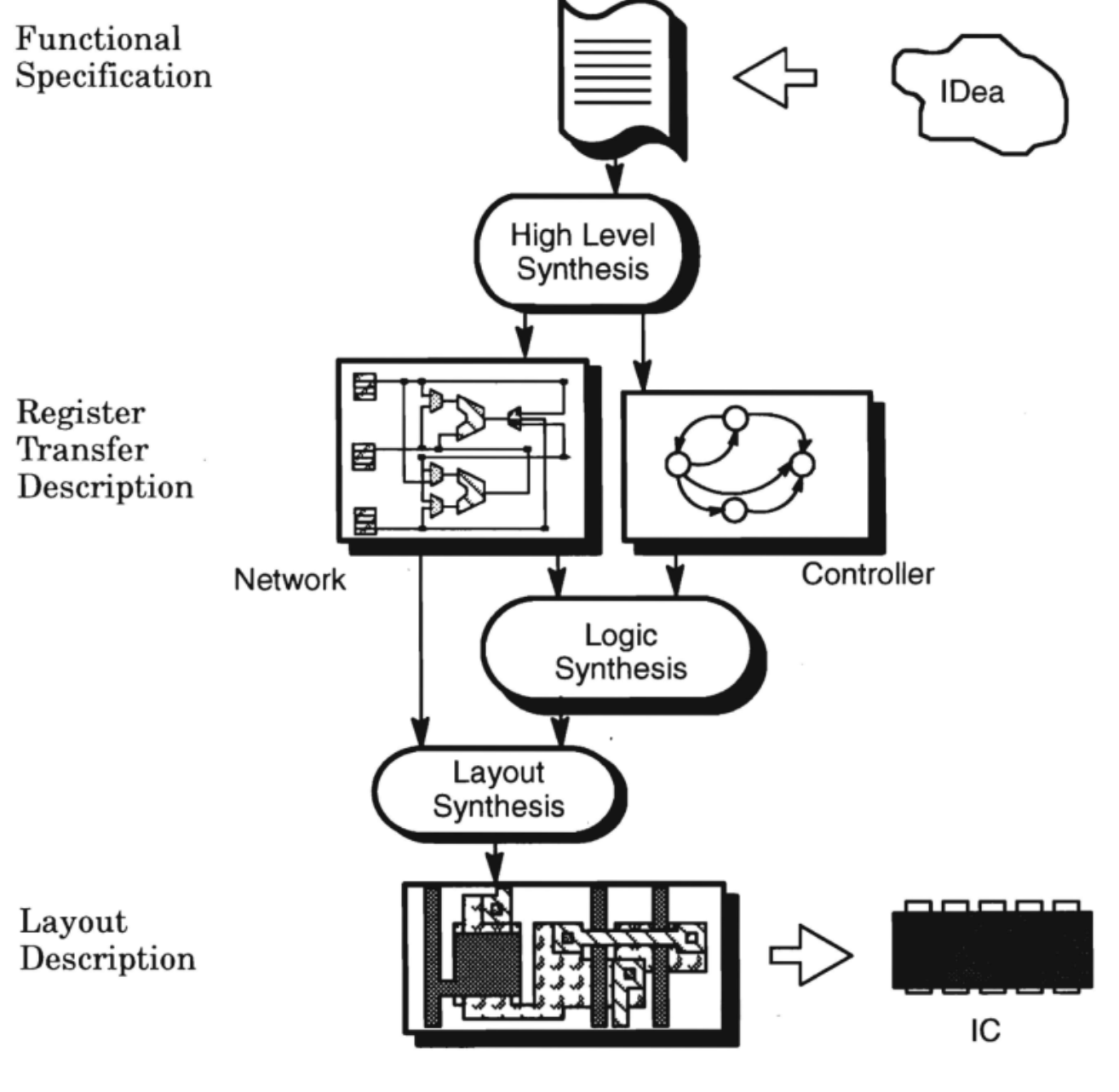
This small marvel enables an unimaginable array of complex functionalities. But did you know that the birth of such a "magical" chip is the culmination of dedicated efforts from countless VLSI (Very Large Scale Integration) engineers? Specifically, the RTL-to-GDSII (RTL2GDS) process is the core, the very flower, of semiconductor development, transforming abstract ideas into tangible silicon.
The RTL Engineer: From Idea to Code, The Genesis of Digital Circuit Design
RTL (Register Transfer Level) Engineers stand at the forefront of digital circuit design, defining its functionality and implementing it using Hardware Description Languages (HDL). Much like an architect drafting a building's blueprint, they create the logical master plan for the chip's functions and operational methods. Every line of code we write forms the chip's backbone, dictating the final product's performance and capabilities, thus carrying immense responsibility.
In some companies(usually startups. They are called by 'ASIC Front-end Engineer'), an RTL engineer might handle everything from algorithm development, FPGA design, and IP core design to SoC integration, generating SDC (Synopsys Design Constraints) and UPF (Unified Power Format) for Logic Synthesis, and even testbench creation.
Conversely, in other companies, each of these steps might be handled by a separate dedicated engineer. This shows how the scope of an RTL engineer's role can flexibly adapt based on company culture and project specifics.
An RTL engineer's day is typically filled with the following tasks:
- Wrestling with Specifications: Understanding and QuestioningEvery design begins with the Specification. It's crucial to thoroughly read and understand this document, which outlines customer requirements and overall system demands. This process is like deciphering a complex map, requiring meticulous attention to every small detail. Sometimes, the specification itself might be ambiguous or incomplete. In such cases, RTL engineers delve into the core of the spec, contemplating how to translate it into a feasible design. They also meticulously organize and communicate questions to the design, system, or even customer teams to eliminate any room for misunderstanding. Clarity at this initial stage profoundly impacts the efficiency of all subsequent processes.
- Design and Code Writing: Bringing Logic to Life, While OptimizingOnce the specification is clear, the real work of writing RTL code in languages like Verilog or SystemVerilog to define hardware behavior begins. This code isn't merely about implementing functionality; it must be designed with future performance (speed), power efficiency, and area (chip size) in mind. For instance, they consider whether to process certain functions in parallel, how to structure the pipeline, and embed optimized logic into every line of code. Initial errors are filtered out by performing basic tests using simulation tools (e.g., Synopsys VCS, Cadence Xcelium) to ensure the written code behaves as expected.
- Collaboration: Refining Design Through Constant CommunicationDesign is never a solo endeavor. Code reviews with team members are essential to ensure the design is heading in the right direction, nothing has been missed, and there are no more efficient approaches. Furthermore, cross-team meetings with Verification and Physical Design teams are indispensable. They incorporate requirements from the Verification team to enhance verifiability and discuss potential constraints during placement and routing (e.g., module size, port locations, clock frequencies) with the Physical Design team, integrating these into the design upfront. Flexibility in embracing and implementing feedback is crucial at this stage. Sometimes, such feedback can significantly alter the initial design direction, but ultimately, it's a process that leads to a more robust and efficient chip.
- Problem Solving: A Cycle of Debugging, Correction, and Brave FECOsDiscovering bugs during simulation is almost an occupational hazard for RTL engineers. They use EDA tools to debug, analyze the root cause of issues, and make corrections. When a bug is found, they must act like detectives, meticulously tracing the logical path to uncover its origin. Occasionally, simply modifying the RTL code isn't enough, and they might have to request a FECO (Front-End Change Order) from the Physical Design team. The phrase, "I'm sorry, but just one FECO..." carries the weight of countless hours of debugging and deliberation. While design changes significantly impact physical implementation and must be approached cautiously, they are sometimes unavoidable and can be the last resort for problem resolution.
- Learning and Development: The Imperative of Continuous Self-ImprovementSemiconductor technology is constantly evolving, with new standards and methodologies emerging. Staying updated by studying new design techniques and methodologies through the latest papers, tech blogs, industry seminars, and vendor-provided training materials is a critical part of an RTL engineer's job. They revisit ongoing designs to identify areas for improvement and play a mentoring role, advising junior engineers and helping them grow technically. Upgrading and sharing the team's technical stack not only fosters individual growth but also strengthens the entire team's capabilities.
- Scripting and Automation: Masters of Efficient Work Environments reduce repetitive and time-consuming tasks and boost productivity. RTL engineers write and refine scripts using languages like Perl, Python, and Tcl. They leverage automation tools for simulation execution, results collection, log analysis, and report generation, maximizing work efficiency. This not only saves time but also significantly reduces human error and ensures consistency in operations. Proficient scripting skills are a hidden asset for an RTL engineer.
- Long-Term Goals and Collaboration: Harmonizing the SystemBeyond simply designing individual blocks, RTL engineers integrate their RTL blocks with those from other teams (e.g., CPU cores, memory controllers, interface IPs) to harmonize the entire system. They perform pipeline verification to ensure the design fits the overall data flow and undertake design optimization to mitigate performance bottlenecks. This is a crucial process for ensuring the overall system efficiency in complex SoC (System on Chip) environments.
An RTL engineer's day involves managing every stage from design initiation to completion, growing and facing challenges through close collaboration with the team. Their collective efforts led to the crucial milestone for the SVP (Silicon Validation Phase): RTL Freeze. An RTL Freeze signifies that no more RTL code changes will occur, serving as an essential commitment before proceeding to the Physical Design phase.
The Design Verification Engineer: The Relentless Pursuers of Bugs, Ensuring Design Quality
Design Verification (DV) Engineers are responsible for ensuring that the RTL design functions as intended, serving as the 'quality assurance' for the design. They focus on finding and fixing potential bugs to guarantee the final product's reliability. Since the mid-2010s, demand for DV roles has exploded, reflecting the high level of expertise and complexity required in this field. Much like a QA team for software development, DV engineers are accountable for the quality of hardware design.
There's a common saying that DV engineers are sometimes "verification engineers (or design fill-ins in emergencies)," highlighting their close interaction with RTL engineers and their need for deep design knowledge. They don't just run test cases; they must understand the design's intent and anticipate unforeseen scenarios to 'hunt' for bugs.
And.. there is a huge demand for DV engineers in the industry. Usually, in bachelor programs, only RTL design is taught, so the supply for DV is relatively small. :)
Here's what a DV engineer's day looks like:
- Deep Understanding of Specifications: Grasping the Design's IntentThoroughly reading and understanding the Specification—which explains how the design should function—is paramount. This process can feel almost artistic in its demands. Hardware designs comprise complex IPs (Intellectual Property) like CPUs, GPUs, memory controllers, and various interfaces, so understanding all related specifications and their interactions takes an enormous amount of time. It often feels like "new tasks are created faster than existing documents can be read," reflecting the sheer volume of information they must digest. A perfect grasp of the designer's intent is essential for building a flawless verification environment.
- Design Analysis: Penetrating the Verification Target, engineers meticulously analyze the design structure of the circuit block currently under verification. This involves poring over RTL code, design documents, and architectural diagrams to gain a complete understanding of each module's functionality, internal operations, and interfaces. They don't just skim the surface; they delve deep into the design's intricacies to pinpoint potential vulnerabilities. This profound understanding at this stage is indispensable for formulating effective test scenarios later on.
- Planning and Coordination: Crafting a Strategic Verification RoadmapThey strategically formulate a Verification Plan, outlining how tests will be conducted. This includes defining test items, coverage goals (e.g., Code Coverage, Functional Coverage), and resource allocation. They also develop realistic plans by considering available computing resources and project timelines, continuously refining and optimizing them as needed. It's akin to a commander strategizing for battle.
- Collaboration and Reporting: Maximizing Synergy Through Transparent CommunicationWeekly/Daily meetings are crucial for transparently sharing progress, identified issues, and future plans with team members. Since verification requires close collaboration with design, DFT, and system teams, cross-team meetings are indispensable. For example, if a bug is found, they report it to the design team, investigate the cause, and jointly seek solutions. Additionally, they create testbench architecture documentation to help team members and related departments easily understand the verification environment. Effective communication minimizes bottlenecks in the verification process and accelerates overall development speed.
- Mentoring and Process Improvement: Knowledge Sharing and Efficiency GainsMentoring junior team members on verification methodologies, UVM (Universal Verification Methodology) usage, and tool operations is vital for the DV team's continuous growth. Furthermore, they analyze existing verification processes and propose efficient verification methodologies to enhance team productivity. They identify new automation techniques and verification efficiency improvements to elevate the entire team's capabilities.
- Learning and Code Review: Staying Current and Upholding QualityDV engineers stay current with the latest trends by reading cutting-edge papers from industry conferences like DVCon (Design and Verification Conference), exploring new verification techniques, and tool utilization strategies. They also perform code reviews of test code written by other team members, proposing improvements and enhancing the overall code quality and consistency across the team. This activity not only boosts individual expertise but also strengthens teamwork.
- Debugging and Scripting: Problem-Solving Prowess and the Power of AutomationAnalyzing and resolving bugs in RTL (Register Transfer Level) designs is a core responsibility of DV engineers. The process of analyzing simulation waveforms and tracing back to the bug's origin demands high-level logical reasoning and persistence. Additionally, they write scripts (Perl, Python, Tcl, etc.) to automate repetitive tasks such as test execution, results analysis, and report generation, thereby increasing efficiency.
- Test Creation and Environment Setup: The Artisans of Robust Verification Environments engineers write test cases and sequences to verify specific behaviors of the design. They employ advanced verification languages and methodologies like UVM (Universal Verification Methodology) and SystemVerilog to build structured test environments (Testbenches) and implement necessary modules (e.g., transactors, scoreboards, drivers, monitors). The goal is to create an environment that closely mimics the real chip's operational conditions, exposing as many potential bugs as possible.
- Querying EDA/IP Vendors: Sometimes, Vendors Are Our PartnersWhen unexpected behavior or bugs are discovered in EDA tools or specific IPs (Intellectual Property) they use, DV engineers contact the respective vendors to inquire and collaborate on issue resolution. Reports like "This seems like a bug...", "Tool crashed," or "Library behavior is odd" contribute to improving the tools' completeness. Sometimes, technical meetings with vendors also provide opportunities to learn about new features or utilization strategies.
- Observing the CI Pipeline: Witnessing the Fruits of AutomationMonitoring the automated build and test process of their code within the CI (Continuous Integration) pipeline is a crucial feedback loop for DV engineers. They review test results and coverage reports to determine the direction of their next tasks, continuously monitoring through regression tests to ensure no new bugs have been introduced into existing functionalities. As the phrase "staring blankly at Teams/Outlook" suggests, analyzing countless logs and test results is also part of their daily routine.
DV engineers play a critical role in ensuring the robustness of designs through meticulous and analytical thinking. Without their persistent efforts, even the most brilliantly designed RTL would not result in a reliable product.
The DFT Engineer: Mastering Testability, The Unsung Heroes of Manufacturing Yield
DFT (Design For Testability) Engineers are specialists responsible for designing semiconductor chips in a way that makes it easy to test for and diagnose defects that might occur during manufacturing. Their role is incredibly important for ensuring chip yield and securing product quality. Given the nature of advanced manufacturing processes, defects are inevitable in mass-produced semiconductors. DFT engineers design 'test highways' within the chip beforehand, making it efficient to locate and diagnose these defects.
The Roles & Responsibilities (R&R) of a DFT engineer also vary by company. Some might only handle DFT logic insertion and ATPG (Automatic Test Pattern Generation), while others engage in a broader range of tasks, from defining DFT specifications, generating STA (Static Timing Analysis) SDCs for DFT, performing Pre/Post-Gate Level simulations, and even conducting board tests and defect diagnosis analysis after the physical chip is produced, down to managing SCAN Restructure/Re-ordering during the P&R (Place & Route) stage. Covering such a wide range of responsibilities, DFT engineers are key personnel situated at the intersection of design and manufacturing.
There is a severe shortage of DFT engineers in Korea 2025. So it is the easiest to get a job in this field. Is TC good? That's another story..........
Here's a glimpse into a DFT engineer's day:
- Morning: Meeting Specifications and Formulating Test StrategiesThe day begins with a deep analysis of customer requirements and the RTL design structure provided by the RTL design team. Based on this, they decide which test techniques (e.g., scan test, BIST, boundary scan) to apply and what fault coverage targets to aim for, formulating an optimal test strategy. They collaborate with the design and verification teams to discuss test strategies and design constraints, anticipating potential issues early on. The strategy established at this stage serves as the blueprint for all subsequent DFT work.
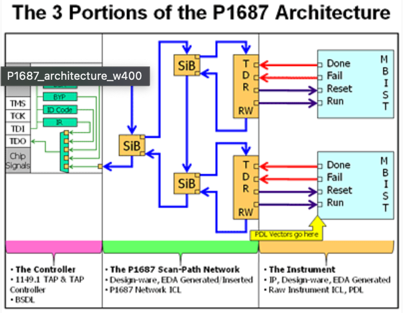
- Designing Test Architecture: Structuring the Chip for Testability engineers design how to efficiently place scan chains within the chip. A scan chain connects all sequential elements (like flip-flops) into one large shift register, allowing test patterns to be easily injected from the outside and results to be read out. They also design and insert BIST (Built-In Self Test) logic, which enables the chip to perform self-tests. For large blocks like memories, they integrate Memory BIST (MBIST) to provide internal self-testing capabilities. They perform SCAN Insertion and Stitching to integrate DFT logic into the RTL design and verify that the added logic does not cause any problems to the overall design, ensuring it's functionally correct and doesn't introduce timing issues.
- Collaboration and Problem Solving: The Synergy with the PD TeamDFT engineers work closely with RTL Designers, Verification Engineers, and Physical Design Engineers to resolve constraints that arise during DFT insertion. For instance, inserting DFT logic can increase gate count, introduce timing violations, or impose layout restrictions. In such situations, a DFT engineer might gingerly approach a PD engineer, saying, "I'm sorry, but just one FECO... if we disconnect this pin and put it into this MUX, it should work..." To which the PD engineer might respond with a complex explanation like, "No, if you put that in, you have to consider its location, the skew won't match, timing will be off, we'll have to re-legalize, re-PV, etc., etc...." Navigating these discussions and finding optimal solutions by reconciling different team perspectives is crucial. Debugging and analyzing simulation results to identify and resolve the root cause of errors are also vital tasks. Furthermore, coordinating with the manufacturing facility (Foundry) regarding test pattern generation and application is an essential part of the job, as they must ensure pattern formats are compatible with the foundry's test equipment.
- Test Pattern Generation: The Core Task of Finding DefectsThey use DFT software (e.g., Synopsys Testmax, Mentor Tessent) to generate optimal ATPG (Automatic Test Pattern Generation) patterns capable of finding defects. ATPG aims to achieve maximum fault coverage with a minimum number of patterns, based on various fault models like stuck-at faults and transition faults. They analyze the fault coverage to ensure the generated test patterns sufficiently test all areas of the design and optimize the patterns for shorter test times and higher efficiency. Generating and managing millions of test patterns is one of a DFT engineer's core competencies.
- Leveraging Tools and Scripting: Automated Efficiency DFT engineers actively utilize EDA tools to automate DFT insertion, ATPG, coverage analysis, and other test-related tasks. They write and refine scripts using scripting languages like Python and Tcl to automate test data processing, results analysis, and report generation. This automation is crucial for efficiently managing complex DFT processes and minimizing human errors.
- Verification and Reporting: Analyzing Results and Proposing ImprovementsThey perform simulations with the generated test patterns (e.g., gate-level simulation) and analyze the test results to identify areas with insufficient test coverage. Preparing reports summarizing the progress for each block, achieved fault coverage, and future improvement directions is also a critical task. These reports serve as important indicators of the product's manufacturability and quality.
- Learning and Mentoring: Continuous Growth and Knowledge TransferStaying current with the latest DFT techniques (e.g., improved diagnostic accuracy, low-power DFT) and methodologies by reading new papers, attending seminars, and reviewing technical documents is essential for enhancing an engineer's capabilities. They also mentor new team members, explaining basic DFT concepts and tool usage, and propose process improvement ideas to boost team efficiency.
DFT engineers are the unsung heroes who directly ensure a chip's manufacturability and quality. Without their efforts, even the most well-designed chip could face severe yield issues during mass production.
The Physical Design Engineer: The Master of Silicon, Bringing Logic to Life
Physical Design (PD) Engineers are the specialists who transform the RTL design created by the RTL design team into an actual physical chip. They are like urban planners, meticulously arranging and connecting billions of transistors and wires within the chip in an optimized layout for efficiency and performance. Their work is crucial for optimizing electron flow and meeting the chip's Performance, Power, and Area (PPA) requirements. A PD engineer's day is filled with precise yet arduous tasks, converting abstract digital design concepts into concrete silicon layouts.
There are so many jobs, so many people doing PD work. Give up WLB. This job is not busy 24 hours a day, but each tool runtime is the longest. If you want to get paid a lot, go to CPU or GPU Team.
- Morning: Design Comprehension and Goal SettingThe day begins with a deep dive into the RTL design's logical structure provided by the RTL team, identifying key requirements and constraints. Beyond just understanding the code, they must fully grasp the functionality, block interdependencies, and overall system intent. Simultaneously, they set concrete PPA targets, including the chip's target frequency (performance), allowable power consumption, and final chip size. They collaborate with other teams like DFT and Verification to discuss the overall design flow and constraints, anticipating potential issues during physical implementation. This initial 'insight' is pivotal for guiding all subsequent optimization efforts.
- Preparing Design Data: Sketching the Blueprint for ImplementationPD engineers establish the entire RTL-to-GDSII flow that translates the logical design into a physical silicon layout. This complex process involves the synergistic operation of various EDA tools and scripts. They verify the standard cell, memory macro, and I/O pad libraries specific to the semiconductor manufacturer's process technology and set up the initial work environment. Crucially, they accurately prepare constraint files (SDC: Synopsys Design Constraints) that reflect critical design requirements like clocking, reset, and data transfer timings. An error in the SDC can prevent even the most advanced tools from yielding correct results. They also prepare UPF (Unified Power Format) files to define the power supply network.
- Placement and Routing: Building the Chip's City and Paving Its Roads
- Floorplanning: This is the stage where the big picture of the entire chip is laid out. They determine the size and location of major IPs like CPU cores, memory, and various interface blocks, ensuring efficient communication paths between them. It’s like zoning a city, arranging blocks to optimize area and performance.
- Power Network Design: PD engineers design the power grid to ensure a stable power supply to the chip. Power lines are meticulously placed and connected to minimize IR Drop (voltage drop) and EM (Electromagnetic Interference).
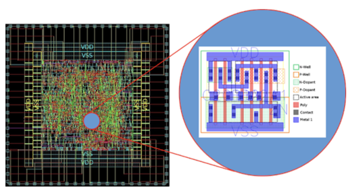
- Placement: Within the floorplanned space, billions of standard cells are placed in optimal locations. This highly complex stage involves EDA tools automatically placing hundreds of millions of cells, taking into account timing constraints, power consumption, and area, combined with the PD engineer's seasoned expertise.
- Clock Tree Synthesis (CTS): This crucial step involves designing the clock tree to efficiently distribute the clock signal, ensuring all digital circuits on the chip operate synchronously. The primary challenge is to minimize Clock Skew (the difference in arrival times of the clock signal to various parts of the chip) and meet Clock Latency targets.
- Routing: All logical connections (Nets) between placed cells are converted into physical metal interconnects. This requires meticulously connecting every line while satisfying timing, area, and power constraints, often utilizing dozens of metal layers and vias to complete the intricate circuit.
- Timing and Verification: The Make-or-Break Stage for Chip Functionality determines whether the chip will function correctly and, more importantly, whether it will be competitive in the market.
- STA (Static Timing Analysis): They statically analyze the signal propagation delay across all paths in the chip to ensure it meets the designed clock frequency (performance) targets. Even a single Timing Violation can prevent the chip from functioning correctly. PD engineers tirelessly identify and resolve countless violations by continuously optimizing the design.
- Power Analysis: They analyze the chip's power consumption and devise strategies to improve power efficiency. Both static and dynamic power consumption are considered to ensure that low-power design goals are met.
- EM/IR Analysis: In high-performance chips, electromagnetic interference (EM) and voltage drop (IR Drop) across power lines can cause serious problems. EM/IR analysis helps predict and mitigate these phenomena, ensuring the stability of power signals.
- DRC (Design Rule Check) / LVS (Layout Versus Schematic) Verification: DRC verifies that the design adheres to manufacturing process rules (e.g., line width, spacing, via size). This determines if the chip can be physically fabricated. LVS verifies that the final layout logically matches the RTL (or netlist). Both verifications must pass perfectly before the chip is ready for manufacturing. If errors are found here, the chip either won't function or will be defective.
- Problem Solving and Collaboration: A Continuous Process of RefinementAnalyzing and resolving issues discovered during verification, such as timing violations, power problems, placement errors, and routing DRC/LVS violations, is a primary responsibility of PD engineers. They leverage cutting-edge EDA tools like Synopsys ICC2 and Cadence Innovus to automate tasks and boost efficiency. Through continuous discussions with RTL, DFT, and Verification teams, they improve design quality, understand each other's constraints, and produce optimal results. Particularly when timing issues arise, they might request a FECO from the RTL team or discuss SCAN Re-ordering with the DFT team, highlighting the necessity of flexible inter-team collaboration.
- Design Optimization: Finding the PPA BalancePerformance, Power, and Area are three critical factors that often involve trade-offs. PD engineers iteratively adjust and optimize the design to balance these three objectives. When design changes occur, they incorporate them via an ECO (Engineering Change Order) to refine the design's completeness down to the last detail. Sometimes, a small change can significantly improve the entire chip's performance. They analyze how well the design has achieved its initial goals and plan further improvements to deliver the best possible outcome.
- Final Stage: GDSII Generation and Tapeout PreparationOnce all verifications are perfectly complete, the GDSII file—the actual design data used for manufacturing—is generated. GDSII is the standard format used in semiconductor manufacturing processes to pattern the circuit onto the wafer. When this file is delivered to the manufacturing facility (Foundry), 'Tapeout' is complete, and chip production can begin. Documenting the final design process and results for the team and clients is also crucial. However, this might not always be the end. If a serious issue arises during manufacturing, or if a last-minute design change is necessary, a Metal ECO might be performed before the BEOL (Back-End-of-Line) process begins, requiring a new update of the BEOL circuit diagram to the foundry. While this is a rare and arduous process, it's a final effort to prevent the production of faulty chips.
A PD engineer's day is a critical journey of overcoming all challenges in transforming a logical design into a physical reality, ultimately ensuring the chip's success. Without their dedication and hard work, no chip could ever come into existence.
Conclusion: Collaboration, The Cornerstone of VLSI's Future
RTL, Verification, DFT, and Physical Design engineers each play a unique and indispensable role. Yet, their efforts interlock like the precise gears of a watch. The RTL engineer lays the design's foundation, the Verification engineer ensures its robustness, the DFT engineer builds in testability, and finally, the Physical Design engineer brings it all to life on silicon. The countless challenges and obstacles encountered throughout this process cannot be overcome alone; they demand meticulous communication and organic collaboration.

![[STA] Synchronous Clocks vs. Asynchronous Clocks](https://images.unsplash.com/photo-1533749047139-189de3cf06d3?crop=entropy&cs=tinysrgb&fit=max&fm=jpg&ixid=M3wxMTc3M3wwfDF8c2VhcmNofDF8fGNsb2NrfGVufDB8fHx8MTc1NTQzMzg1OHww&ixlib=rb-4.1.0&q=80&w=600)

