VLSI Blog
  • Home
  • About
  • VLSI Korea
  • K-Career Community
Sign in Subscribe

Chase Na

Chase Na
Memory Hierarchy & Memory Wall

Memory Hierarchy & Memory Wall

Key Takeaway: From 1947’s magnetic core memory to the forthcoming HBM4 and compute-in-memory architectures, advances in semiconductor memory have continuously reshaped computing performance, capacity, and architecture. Understanding detailed memory types—from on-chip SRAM variants to emerging non-volatile memories—is essential for engineering high-performance, cost-effective systems. 1. Fundamental Principles of

By Chase Na 26 Sep 2025
[STA] Synchronous Clocks vs. Asynchronous Clocks

[STA] Synchronous Clocks vs. Asynchronous Clocks

In the world of digital design, you often hear the terms synchronous clock and asynchronous clock. While simple designs with a single module might use just one clock, modern Systems-on-a-Chip (SoCs) are typically designed with a variety of asynchronous clocks. For example, let's look at the Qualcomm Snapdragon

By Chase Na 26 Sep 2025
What is Physical Design Rule Checking (Physical DRC)?

What is Physical Design Rule Checking (Physical DRC)?

Physical Design Rule Checking (DRC) is the cornerstone of semiconductor physical verification, ensuring that an integrated circuit’s layout adheres to the foundry’s manufacturing constraints. By automating the validation of geometric and spacing requirements in chip layouts, DRC prevents catastrophic defects—shorts, opens, misalignments—and secures high yields, manufacturability,

By Chase Na 19 Sep 2025
Why is Interconnect Delay Still Large with Advanced Process Nodes?

Why is Interconnect Delay Still Large with Advanced Process Nodes?

The continuous scaling of semiconductor process nodes improves transistor density, but it disproportionately amplifies interconnect parasitics, necessitating a "shift-left" approach where the interconnect effect, particularly resistance, must be considered much earlier and more stringently throughout the design flow. The transition to advanced process nodes signifies a shift from

By Chase Na 12 Sep 2025
What is Library Characterization? feat: SPICE, and Static Timing Analysis (STA)

What is Library Characterization? feat: SPICE, and Static Timing Analysis (STA)

Overview of SPICE and STA In modern high-density VLSI design, it's crucial to ensure that an integrated circuit (IC) operates correctly and reliably at its specified clock period. This is achieved through rigorous timing analysis, which identifies potential performance bottlenecks and ensures compliance with timing constraints. Static Timing

By Chase Na 05 Sep 2025
What is SPEF (Standard Parasitic Exchange Format)?

What is SPEF (Standard Parasitic Exchange Format)?

In the field of Very Large Scale Integration (VLSI) design, a finished semiconductor chip's performance is not only determined by its logical functionality but is also significantly affected by physical phenomena that occur on the tiny wires, or interconnects, inside the chip. These physical phenomena are known as

By Chase Na 29 Aug 2025
What is MPW (Multi-Project Wafer)?

What is MPW (Multi-Project Wafer)?

Multi-Project Wafer (MPW) is a service that allows various semiconductor designs to be fabricated on a single wafer. Think of it like a "variety pizza"—instead of ordering a full pizza with just one topping, an MPW wafer combines multiple different designs from various teams onto a single

By Chase Na 22 Aug 2025
SDC: Why use 60% IO Delay for set_input_delay and set_output_delay?

SDC: Why use 60% IO Delay for set_input_delay and set_output_delay?

Chip design, particularly for modern, complex System on Chip (SoC) designs, is growing on an unimaginable scale. In the past, it was possible to fit an entire design into a single Verilog netlist and process it with an EDA tool. Now, that approach leads to several problems. Massive Designs, New

By Chase Na 17 Aug 2025
Yield, Harvesting Models, and the Foundry Business

Yield, Harvesting Models, and the Foundry Business

Introduction Engineering, unlike pure science, incorporates an additional crucial variable: profitability. The decision to mass-produce semiconductors hinges entirely on whether it can be done profitably. As of 2024/2025, how far have semiconductor manufacturing processes advanced? Are we at 3nm, 2nm, or 1.8nm? We have reached 0.7nm. IMEC

By Chase Na 01 Aug 2025
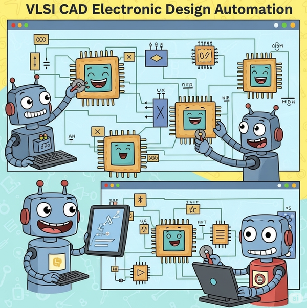
What is VLSI CAD and EDA?: Electronic Design Automation

What is VLSI CAD and EDA?: Electronic Design Automation

All electronic devices that underpin modern society—smartphones, computers, automobiles, AI servers, and more—cannot exist without semiconductor chips. These tiny chips integrate billions of microscopic transistors onto a single piece of silicon, a highly integrated technology known as Very Large Scale Integration (VLSI). VLSI is not merely a continuation

By Chase Na 07 Jul 2025
All Digital Semiconductor Design Role overview: What does that engineer do?

All Digital Semiconductor Design Role overview: What does that engineer do?

Smartphones, cars, and home appliances. The pulsating heart of these advanced devices, nestled in your hand or woven into your daily life, is often a tiny semiconductor chip. This small marvel enables an unimaginable array of complex functionalities. But did you know that the birth of such a "magical&

By Chase Na 06 Jul 2025
What is Tape Out in VLSI?

What is Tape Out in VLSI?

Do you have a semiconductor design engineer in your family? Before planning your Vacance? ask them for their 'Tape out' schedule. The term “tape-out” harks back to the 1970s when engineers recorded design data on magnetic tapes and physically shipped them to foundries (Tapeout Origin). These tapes held

By Chase Na 04 Jul 2025
See all
VLSI Blog
  • Sign up
Powered by Ghost

VLSI Blog

I'll research semiconductors until the day I die. And share everything I learn. [Via mail every week]