Comprehensive Analysis of Semiconductor Yield, Binning, and Defect Level


Introduction to Semiconductor Yield
In Very Large Scale Integration (VLSI) manufacturing, yield is a cornerstone metric that quantifies the proportion of functional integrated circuits (ICs) produced from a silicon wafer. Defined as the ratio of good chips to total chips, yield directly influences the economic viability of semiconductor production. The formula for yield is straightforward:
Y = (Good Chips) / (Total Chips)
A yield of 1 (or 100%) indicates that all chips are defect-free, a rare occurrence in practice. As semiconductor processes advance to smaller nodes (e.g., 5nm, 3nm), the cost of processing a single wafer escalates due to the complexity of fabrication steps, such as photolithography and etching. Consequently, maximizing yield is paramount to minimize the cost per functional chip, calculated as:
Good Die Cost = (Wafer Price / Die Count) * (1 / Y)
This equation highlights that lower yields significantly increase the cost per good die, underscoring yield's role in profitability. For instance, if a wafer costs $10,000 and yields 500 dies with a 50% yield, the cost per good die is $40, compared to $20 at 100% yield.
Factors Influencing Yield
Several factors impact yield, each contributing to the challenges of achieving high production efficiency:
- Defect Density (D): Measured as defects per square centimeter, defect density reflects the quality of the manufacturing process. Sources include material impurities, equipment malfunctions, or environmental contaminants. A lower defect density correlates with higher yield.
- Chip Area (A): Larger chips have a higher probability of containing defects due to their increased surface area, reducing yield. This is particularly relevant for complex processors or GPUs.
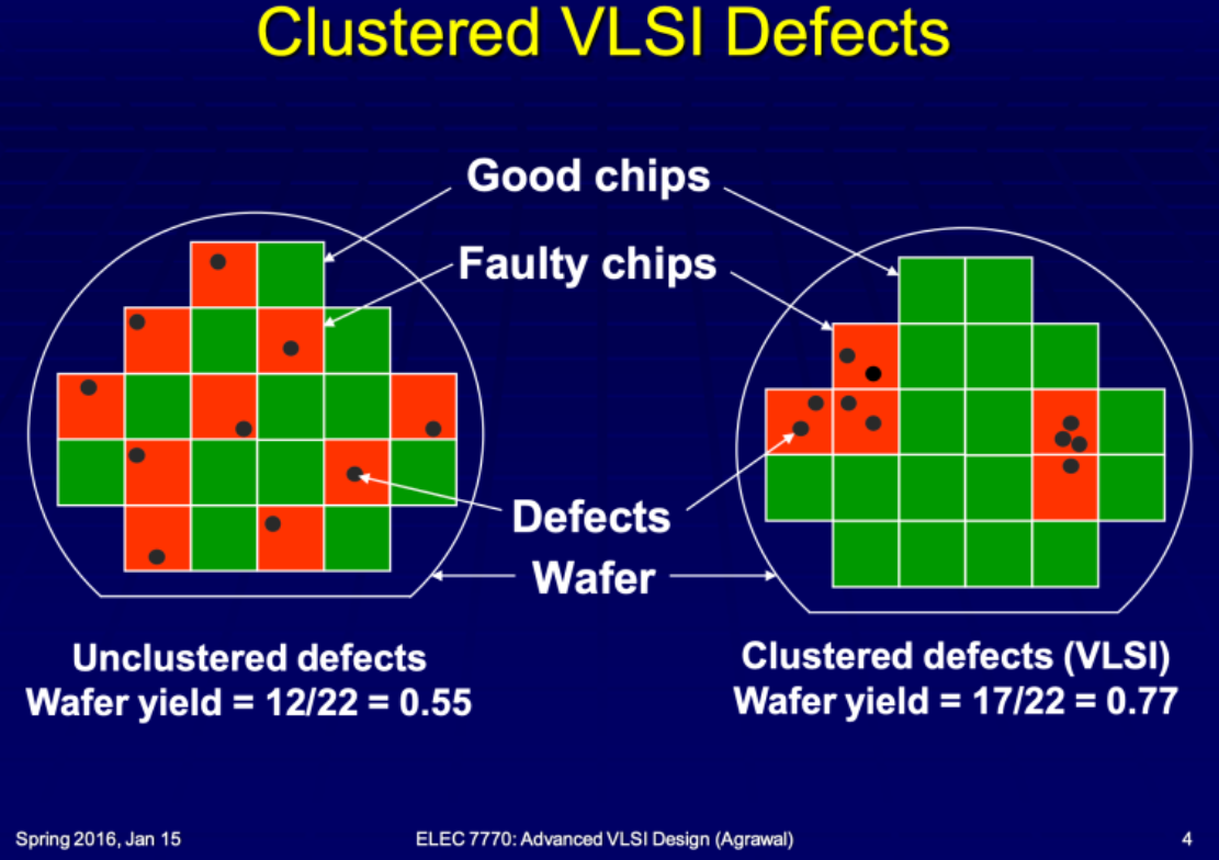
- Fault Clustering: Defects may not be uniformly distributed. Clustered defects, often resulting from specific process issues, can affect fewer dies than random defects, potentially improving yield.
- Process Maturity: New fabrication processes typically start with lower yields, improving as engineers optimize equipment and procedures. Mature processes, like 28nm, often achieve higher yields than cutting-edge 3nm nodes.
These factors interact dynamically, requiring sophisticated models to predict and optimize yield.
Yield Models
To estimate yield, manufacturers rely on mathematical models that account for defect distribution:
- Poisson Model: Assumes defects are randomly distributed across the wafer. The yield is given by:
- Y = e^(-D * A)
- Here, D is the defect density, and A is the chip area. This model is simple but assumes no defect clustering, which may not always hold true.
- Negative Binomial Model: Accounts for defect clustering, common in real-world scenarios. The yield is expressed as:
- Y = (1 + (D * A) / alpha)^(-alpha)
- where alpha is the clustering parameter. A smaller alpha indicates stronger clustering. As alpha approaches infinity, this model converges to the Poisson model. This model is more accurate for modern processes where defects tend to cluster due to systematic issues.
- Murphy’s Model: Another model mentioned in industry literature, it calculates yield as:
- Y = ((1 - e^(-D * A)) / (D * A))^2
- This model assumes a triangular defect density distribution and is useful for specific defect types Statistical Yield Limits.
These models enable manufacturers to predict yield losses and optimize process parameters.
Defects in Semiconductor Manufacturing
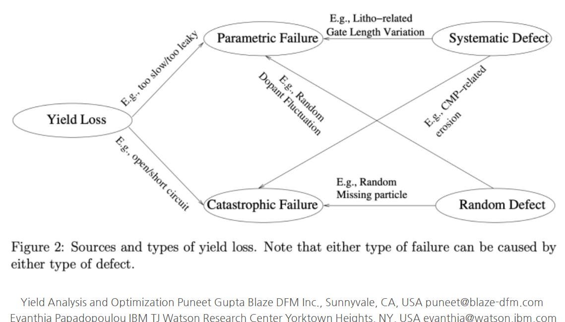
Defects are physical or electrical anomalies that impair chip functionality. They are classified into three types:
- Parametric Defects: Variations in electrical parameters (e.g., threshold voltage, resistance) that deviate beyond acceptable limits, often due to process variations.
- Systematic Defects: Result from design or process issues affecting multiple chips, such as mask misalignment or incorrect etching patterns.
- Random Defects: Unpredictable defects caused by particles or contaminants, distributed sporadically across the wafer.
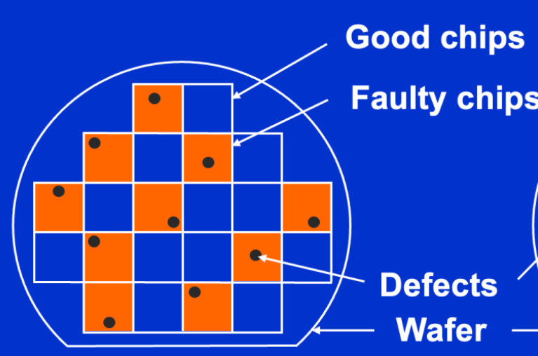
Defect distribution significantly affects yield. Randomly distributed defects impact a larger number of dies, while clustered defects, often from specific process steps, may affect fewer dies, potentially improving yield. For example, a cluster of defects in one wafer region might ruin only a few dies, whereas the same number of random defects could affect many more.
Fault Coverage and Testing
Fault coverage (F) measures the proportion of detectable defects during testing, defined as:
F = (Detected Faults) / (Total Possible Faults)
For instance, if a chip has 3,000 potential faults and testing détects 500, the fault coverage is:
F = 500 / 3000 = 0.1667 or 16.67%
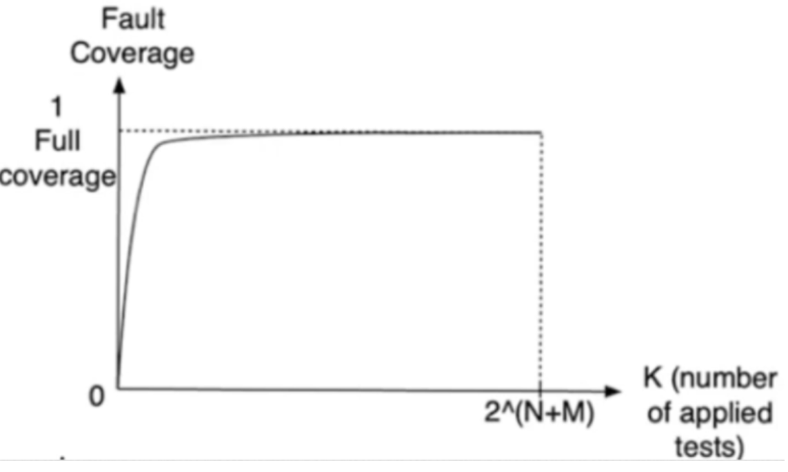
High fault coverage is desirable to ensure defective chips are identified, but achieving 100% coverage is impractical due to the exponential increase in testing time and cost. Fault coverage typically rises quickly with initial test patterns but saturates, as remaining faults are harder to detect. Industry often targets 95–99% coverage to balance quality and time-to-market Fault Coverage.
Testing involves applying test patterns to identify faults, often using standards like IEEE 1149.1 (JTAG) for boundary scan testing. However, untestable defects exist, necessitating design-for-test (DFT) techniques to enhance fault detection.
Defect Level (DL)
Defect level represents the proportion of defective chips that pass testing and are shipped, measured in parts per million (ppm). It is a critical quality metric, especially for applications requiring high reliability. The Williams-Brown formula relates defect level to yield and fault coverage:
DL = 1 - Y^(1 - F)
where Y is the yield, and F is the fault coverage. For example, with a yield of 80% (Y = 0.8) and fault coverage of 95% (F = 0.95), the defect level is:
DL = 1 - 0.8^(1 - 0.95) = 1 - 0.8^0.05 ≈ 0.011 or 11,000 ppm
This high defect level indicates a need for improved testing. Industry standards vary:
| Application | Defect Level (ppm) |
|---|---|
| General Commercial | ~500 |
| Mature Process | ~100 |
| Aerospace/Military | <30 |
Low defect levels are critical for sensitive applications, where even a single failure can be a catastrophic Defect Level.
Strategies for Yield Improvement
To enhance yield and reduce defect levels, manufacturers employ several strategies:
- Binning: Chips are sorted based on performance metrics (e.g., clock speed, power consumption). High-performing chips are sold as premium products, while others are marketed for less demanding applications, maximizing revenue Techquickie.
- Redundancy and Repair: Incorporating spare circuits, especially in memory chips, allows defective elements to be replaced, improving yield.
- Design-for-Yield (DFY): Designing chips to tolerate manufacturing variations, such as using larger feature sizes or optimizing layouts to avoid critical areas.
- Physical Design Optimization: Minimizing routing congestion and process variation effects through careful layout design, reducing defect susceptibility.
- Post-Silicon Diagnosis: Analyzing failed chips to identify defect causes, informing process and design improvements McKinsey.
Data analytics, including tools like yieldWerx, enable real-time defect identification26 identification and process optimization yieldWerx.
Current Challenges and Trends
Advanced nodes introduce significant yield challenges due to smaller feature sizes and increased process complexity. For example, at 3nm, even minor defects can render chips non-functional, and the cost of a single wafer can exceed $20,000. This necessitates advanced techniques like extreme ultraviolet (EUV) lithography to improve patterning accuracy and reduce defect density.
Moore’s Law, which predicted a doubling of transistor density every two years, is slowing due to yield and cost constraints. The economic implications are profound, with modern fabs costing billions to build and operate. High yields are essential to justify these investments.
Emerging trends include:
- Machine Learning: Predictive analytics to identify defect patterns and optimize processes.
- Advanced Materials: Exploring new materials to reduce defect density.
- Data Visualization: Tools like Pareto analysis and wafer maps to pinpoint yield loss causes DR YIELD.
Conclusion
Semiconductor yield analysis is a complex but critical discipline in VLSI manufacturing. By understanding defect types, employing accurate yield models, optimizing testing for high fault coverage, and implementing yield enhancement strategies, manufacturers can improve profitability and product quality. As the industry pushes toward smaller nodes, innovative approaches will be essential to maintain high yields and meet market demands.
| Metric | Definition | Impact on Manufacturing |
|---|---|---|
| Yield | (Good Chips) / (Total Chips) | Determines cost per functional chip |
| Defect Density | Defects per unit area | Higher density lowers yield |
| Fault Coverage | (Detected Faults) / (Total Possible Faults) | Balances quality and testing cost |
| Defect Level | Defective chips shipped (ppm) | Critical for reliability in sensitive applications |

![[STA] Synchronous Clocks vs. Asynchronous Clocks](https://images.unsplash.com/photo-1533749047139-189de3cf06d3?crop=entropy&cs=tinysrgb&fit=max&fm=jpg&ixid=M3wxMTc3M3wwfDF8c2VhcmNofDF8fGNsb2NrfGVufDB8fHx8MTc1NTQzMzg1OHww&ixlib=rb-4.1.0&q=80&w=600)

