Memory Hierarchy & Memory Wall


Key Takeaway: From 1947’s magnetic core memory to the forthcoming HBM4 and compute-in-memory architectures, advances in semiconductor memory have continuously reshaped computing performance, capacity, and architecture. Understanding detailed memory types—from on-chip SRAM variants to emerging non-volatile memories—is essential for engineering high-performance, cost-effective systems.
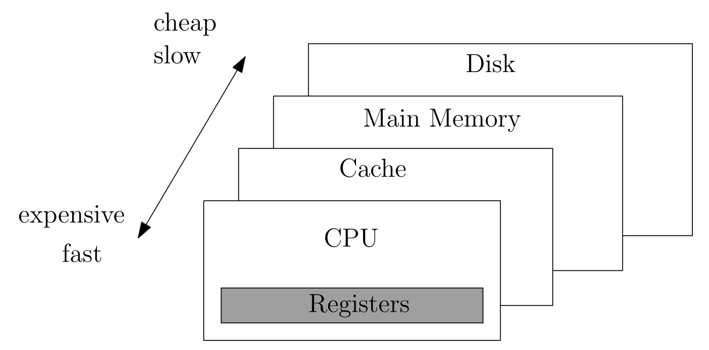
1. Fundamental Principles of Memory Hierarchy
The memory hierarchy leverages the Principle of Locality:
- Temporal Locality: Recently accessed data is likely to be accessed again soon.
- Spatial Locality: Data near recently accessed locations is likely to be accessed soon.
By placing frequently accessed data in faster, more expensive memory and less-frequently accessed data in slower, cheaper memory, systems optimize the trade-off among latency, capacity, and cost.
2. Detailed Memory Semiconductor Types
2.1 On-Chip Memories
[The numbers here are examples.]
CPU Registers
– Latency: 0.25–0.6 ns
– Capacity: < KB
– Technology: Flip-flops (edge-triggered)
– Cost: > $1,000 per GB equivalent
– Usage: Integer and floating-point operands
Static RAM (SRAM)
– Cell: 6-transistor (6T) latch
– Latency: 1–40 ns (varies by level)
– Variants:
- L1 Cache (I-cache/D-cache): 32–64 KB per core, 1–3 ns
- L2 Cache: 256 KB–2 MB per core, 3–10 ns
- L3 Cache (LLC): 8–128 MB shared, 10–40 ns
– Power: Low static leakage, high dynamic switching
– Role: Instruction and data caching for CPU cores
2.2 Off-Chip Volatile Memories
DRAM (Dynamic RAM)
– Cell: 1-transistor, 1-capacitor (1T1C)
– Latency: 50–150 ns
– Variants:
- DDR4: 100–150 ns, 25.6–51.2 GB/s
- DDR5: 80–120 ns, 51.2–76.8 GB/s
- LPDDR: Low-power variant for mobile, ~60–100 ns
– Capacity: 8 GB–256 GB per DIMM
– Cost: $1–5 per GB
– Refresh: Periodic refresh required
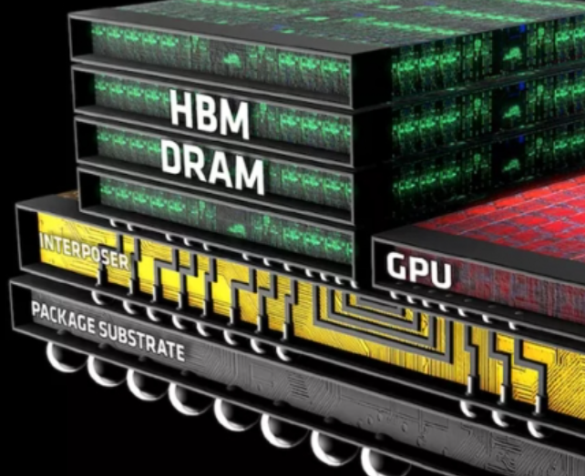
High Bandwidth Memory (HBM)
– Technology: TSV-based 3D stacked DRAM
– Latency: 50–100 ns
– Bandwidth: 1.2 TB/s (HBM3E), 2 TB/s projected (HBM4)
– Capacity: 8 GB–64 GB per stack
– Cost: $5–10 per GB
– Usage: GPUs, AI accelerators, high-performance computing
2.3 Non-Volatile and Emerging Memories
NAND Flash
– Cell: Floating-gate or charge-trap MOSFET, multi-level cell (MLC/TLC/QLC)
– Latency: 10–100 µs
– Capacity: 128 GB–2 TB per die
– Cost: $0.10–0.50 per GB
– Usage: SSDs, embedded storage
3D XPoint (Intel Optane)
– Technology: Phase-change memory (PCM) crosspoint array
– Latency: ~10 µs
– Capacity: 128 GB–512 GB
– Cost: $5–20 per GB
– Role: Storage-class memory bridging DRAM and NAND
Storage-Class Memory (SCM)
– Example: Intel Optane DC Persistent Memory
– Interface: DIMM form factor, memory mapped
– Latency: 500 ns–2 µs
– Cost: $10–20 per GB
– Feature: Byte-addressable non-volatility
Magnetoresistive RAM (MRAM)
– Cell: Magnetic tunnel junction (MTJ)
– Latency: 10–30 ns
– Endurance: > 10^15 writes
– Use cases: Embedded cache, instant-on systems
Resistive RAM (ReRAM)
– Cell: Metal-oxide switching
– Latency: 10–100 ns
– Prospects: Neuromorphic computing, high-density storage
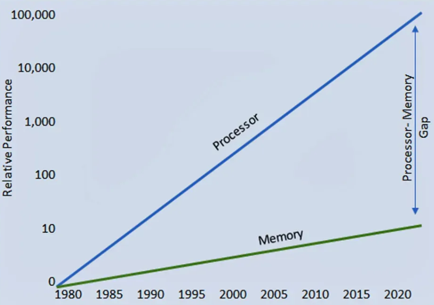
3. Memory Wall: Bottleneck in Performance Scaling
As CPU and accelerator logic speed have improved exponentially under Moore’s Law, memory access speed has lagged, creating the “memory wall”. Data movement now dominates energy consumption—moving a byte costs 10–100× more energy than computing an operation.
4. Strategies to Overcome the Memory Wall
4.1 Advanced Packaging and Interconnects
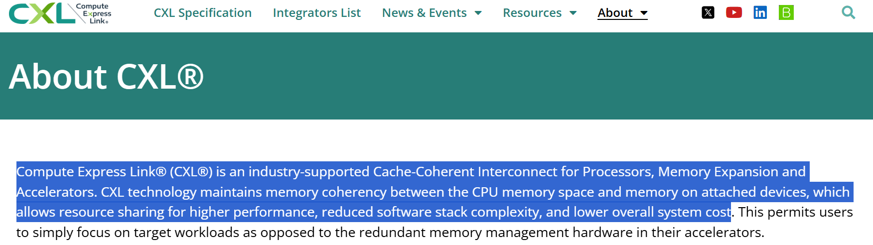
- Compute Express Link (CXL):
– Enables coherent memory pooling across CPUs, GPUs, and accelerator cards
– Allows dynamic allocation of DRAM/CXL memory to hosts
4.2 In-Memory and Near-Memory Computing
- Processing-in-Memory (PIM):
– Embeds programmable compute units adjacent to DRAM arrays
– Reduces data movement, achieves up to 4× performance with 70% energy savings
4.3 3D Monolithic and Heterogeneous Integration
- Monolithic 3D DRAM:
– Cell-level stacking to eliminate TSV bottlenecks, target 10× density gain
- Hybrid Memory Cube (HMC) Successors:
– Integration of logic layers and DRAM for AI accelerators
5. Future Outlook and Strategic Implications
By 2030, over 50% of DRAM revenue is expected from HBM-style products, driving a shift from von Neumann toward memory-centric architectures. Engineers and system designers must:
- Master the full spectrum of memory technologies—from on-chip SRAM variants to emerging non-volatile memories.
- Select optimum memory combinations tailored to workload locality and bandwidth demands.
- Leverage advanced interconnect and in-memory computing to minimize data movement bottlenecks.
In the AI and HPC era, memory is not merely storage but an active computational partner. Strategic adoption of HBM, CXL pooling, PIM/CIM architectures, and cutting-edge non-volatile memories will determine the competitive edge in next-generation computing systems.
![[STA] Synchronous Clocks vs. Asynchronous Clocks](https://images.unsplash.com/photo-1533749047139-189de3cf06d3?crop=entropy&cs=tinysrgb&fit=max&fm=jpg&ixid=M3wxMTc3M3wwfDF8c2VhcmNofDF8fGNsb2NrfGVufDB8fHx8MTc1NTQzMzg1OHww&ixlib=rb-4.1.0&q=80&w=600)


