Strategic Foundry Selection for Next-Generation ASIC Projects: A Comprehensive Engineering Guide


The landscape of semiconductor manufacturing has evolved into a complex ecosystem where foundry selection represents one of the most critical strategic decisions in ASIC development. As process technologies advance beyond the 3nm node and specialized applications demand increasingly stringent requirements, the foundry selection process has transformed from a simple cost-performance analysis to a multidimensional strategic evaluation encompassing technology maturity, supply chain resilience, and long-term partnership viability.
This comprehensive guide provides a systematic framework for evaluating foundry partners across diverse application domains—from high-performance smartphone processors requiring cutting-edge node capabilities to radiation-hardened aerospace systems demanding decades-long reliability. The methodology presented here addresses modern semiconductor teams' full spectrum of considerations when navigating the increasingly complex foundry landscape.
Understanding the Foundry Ecosystem Landscape
The global foundry market has consolidated around several key players, each with distinct technological strengths, geographical advantages, and strategic focus areas. TSMC dominates advanced node production (3nm and below), Samsung Foundry offers competitive alternatives with strong memory integration capabilities, GlobalFoundries focuses on specialized processes for automotive and IoT applications, and emerging players like Intel Foundry Services are establishing new competitive dynamics.
Understanding this ecosystem requires analyzing current capabilities and long-term strategic positioning. Each foundry's technology roadmap, capital investment priorities, and customer partnership models directly impact project feasibility and long-term success. The semiconductor industry's cyclical nature means that foundry capacity, pricing, and technology availability fluctuate significantly, making timing a critical factor in selection decisions.
Application-Specific Design Requirements Analysis
High-Performance Computing and Mobile Applications
For high-performance applications such as smartphone APs, AI accelerators, and data center processors, the primary focus centers on achieving optimal Power-Performance-Area (PPA) metrics at the most advanced process nodes available. These applications typically require:
Advanced Node Utilization: Leading-edge nodes (3nm, 2nm) provide the transistor density necessary for complex SoC integration while maintaining competitive power envelopes. However, the yield ramp profiles at these nodes introduce significant risk considerations that must be weighed against performance benefits.
Thermal Management Capabilities: Advanced packaging technologies, including through-silicon vias (TSVs), advanced substrate materials, and integrated heat spreaders, become critical enablers for high-performance designs. Foundry partnerships with advanced packaging providers can significantly impact total solution viability.
High-Speed I/O Integration: SerDes capabilities, memory interface performance, and package-level signal integrity become foundry differentiators for high-performance applications requiring multi-gigabit data rates.
Automotive and Industrial Applications
Image recommendation: Automotive semiconductor components in engine bay environment
Automotive semiconductor applications introduce unique requirements that fundamentally alter foundry selection criteria:
Automotive Quality Standards: AEC-Q100 qualification requirements, zero-defect manufacturing expectations, and automotive-specific test protocols require foundries with dedicated automotive production lines and quality systems.
Extended Temperature Range Operation: Automotive applications often require operation from -40°C to +150°C or beyond, necessitating specialized process characterization and qualification data that not all foundries provide.
Functional Safety Requirements: ISO 26262 compliance for safety-critical automotive functions requires foundries capable of providing process-level failure mode analysis, statistical process control data, and long-term reliability modeling.
Supply Chain Traceability: Automotive OEMs require complete supply chain visibility, including raw material sourcing, process step documentation, and long-term availability guarantees extending to 15-20 years.
Aerospace and Defense Applications

Aerospace and defense applications represent perhaps the most demanding foundry selection challenges, requiring specialized capabilities that few foundries can provide:
Radiation Hardness Assurance: Space applications require either radiation-hardened-by-design (RHBD) processes or radiation-hardened-by-process (RHBP) technologies. This typically limits foundry options to specialized providers such as BAE Systems, Microchip (formerly Microsemi), or specific qualified processes from mainstream foundries.
Extended Reliability Requirements: Mission-critical aerospace systems may require 20+ year operational lifetimes without maintenance, necessitating extensive accelerated aging studies and reliability modeling that exceeds commercial requirements by several orders of magnitude.
Security and Supply Chain Requirements: Defense applications often require trusted foundry status, domestic content requirements, and anti-tamper manufacturing processes that significantly constrain foundry options.
Single Event Effects (SEE) Mitigation: Cosmic radiation in space environments can cause single event upsets (SEUs), single event latchup (SEL), and single event burnout (SEB). Foundry processes must be characterized for these effects, and design rules must be available for mitigation strategies.
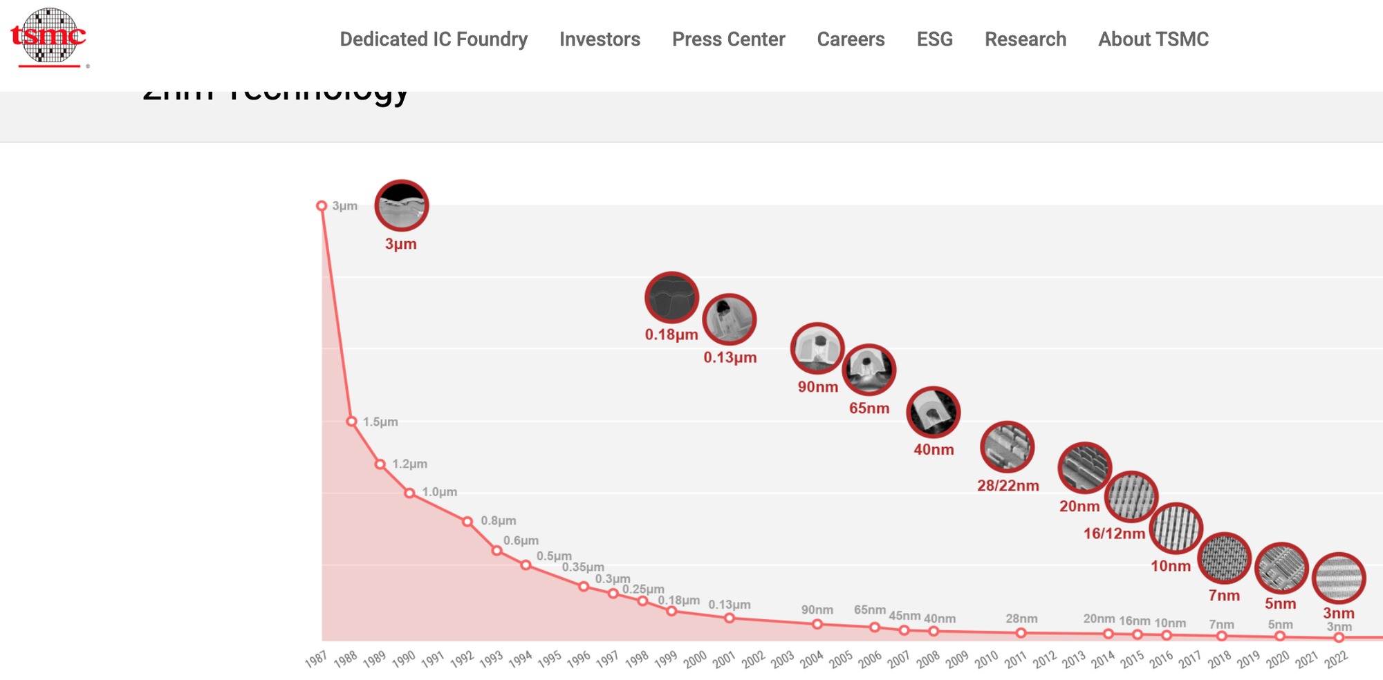
Technology Node Selection Strategy
Advanced Node Considerations (5nm and Below)
Advanced nodes offer compelling advantages in performance and power efficiency but introduce significant complexity and risk factors:
Yield Maturity Timeline: New process nodes typically require 12-24 months to achieve production-worthy yields. Early adopters face higher costs and potential supply disruptions during yield ramp phases.
Design Rule Complexity: Advanced nodes introduce increasingly restrictive design rules, requiring sophisticated EDA tools and design methodologies that may necessitate significant team training and tool investments.
Process Variability Management: As transistor dimensions approach atomic scales, process variations become increasingly significant, requiring advanced statistical design techniques and robust circuit architectures.
Cost Structure Analysis: While advanced nodes offer superior area efficiency for high-transistor-count designs, the mask costs, NRE investments, and minimum order quantities can make them economically unfeasible for lower-volume applications.
Mature Node Optimization (28nm and Above)
Mature process nodes continue to serve critical roles in many applications:
Automotive-Qualified Processes: Most automotive-qualified processes remain concentrated in mature nodes (28nm-180nm) due to the extensive qualification timelines required for automotive applications.
Analog and Mixed-Signal Optimization: Mature nodes often provide superior analog performance characteristics, including better transistor matching, lower 1/f noise, and more predictable device behavior across temperature and voltage variations.
Cost-Optimized Solutions: For price-sensitive applications, mature nodes offer stable pricing, high yields, and proven reliability records that can provide significant cost advantages over advanced nodes.
Specialty Process Integration: Mature nodes often support specialized process options such as embedded flash memory, MEMS integration, and high-voltage transistors that may not be available at advanced nodes.
Process Performance and Reliability Assessment

Comprehensive Yield Analysis
Foundry yield performance directly impacts both cost and delivery predictability. A thorough yield assessment should encompass:
Parametric Yield Analysis: Beyond simple functional yield, parametric yield analysis examines the distribution of key performance parameters (speed, power, leakage) across wafer lots. This analysis reveals process centering, variation control, and the likelihood of meeting design targets across production volumes.
Defect Density Tracking: Historical defect density data provides insights into process maturity and continuous improvement trajectories. Established processes should demonstrate consistent defect density reduction over time, while new processes may show higher initial defect rates with steep improvement curves.
Systematic vs. Random Defects: Understanding the breakdown between systematic defects (caused by design rule violations or process sensitivities) and random defects (particles, equipment malfunctions) helps predict yield improvement potential and identify risk mitigation strategies.
Reliability and Qualification Standards
Long-term reliability becomes increasingly critical as semiconductor devices are deployed in mission-critical applications:
Accelerated Testing Protocols: Comprehensive reliability assessment requires examining foundry capabilities for accelerated testing, including highly accelerated stress testing (HAST), temperature cycling, electromigration testing, and bias temperature instability (BTI) characterization.
Statistical Reliability Modeling: Advanced reliability programs require statistical modeling capabilities to predict failure rates under actual operating conditions based on accelerated test results. This capability varies significantly between foundries and directly impacts the ability to meet strict reliability requirements.
Process Qualification Documentation: Military, aerospace, and automotive applications often require extensive process qualification documentation, including statistical process control data, failure mode analysis, and long-term reliability projections that may not be available from all foundries.
Supply Chain Risk Assessment and Mitigation
The semiconductor industry's global nature introduces complex geopolitical considerations:
Regional Manufacturing Distribution: Over-reliance on any single geographic region introduces supply chain vulnerability. Evaluating foundry manufacturing footprint across multiple regions provides risk diversification opportunities.
Export Control Compliance: Evolving export control regulations affect technology access and supply chain flexibility. Foundry selection must consider current and potential future regulatory constraints that could impact technology availability or supply continuity.
Dual-Source Strategy Development: Critical applications often require dual-source manufacturing capabilities, necessitating foundry partners with compatible processes or migration pathways between different foundries.
Material and Equipment Supply Dependencies
Understanding foundry supply chain dependencies reveals potential vulnerability points:
Critical Material Sources: Certain specialty materials (photoresists, specialty gases, ultra-pure chemicals) may have limited supplier bases, creating potential supply disruption points.
Equipment Vendor Dependencies: Foundries' dependencies on specific equipment vendors (ASML for EUV lithography, Applied Materials for deposition systems) can create capacity constraints during periods of high demand.
Logistics Infrastructure: Semiconductor manufacturing requires complex logistics networks for chemical delivery, waste management, and product shipment. Regional infrastructure capabilities can impact supply chain resilience.
Financial Analysis and Cost Optimization
Total Cost of Ownership Modeling
Comprehensive foundry cost analysis requires examining multiple cost components:
Wafer-Level Cost Structure: Basic wafer pricing provides only a starting point for cost analysis. Additional factors include sort test costs, engineering wafer charges, and volume-based pricing tiers that can significantly impact unit economics.
NRE Investment Analysis: Non-recurring engineering costs encompass mask tooling, process design kit (PDK) licensing, design rule check (DRC) development, and first-silicon engineering support. These costs can range from hundreds of thousands to tens of millions of dollars for advanced nodes.
Hidden Cost Identification: Additional costs often include expedite charges, engineering change order fees, yield enhancement services, and failure analysis support that may not be apparent in initial cost estimates.
Learning Curve Economics: New process technologies typically exhibit learning curve effects where costs decrease as production volumes increase. Modeling these effects helps predict long-term cost trajectories.
Risk-Adjusted Financial Modeling
Financial analysis must incorporate various risk factors:
Yield Risk Quantification: Yield shortfalls directly impact unit costs and delivery schedules. Risk-adjusted financial models should include yield scenarios ranging from best-case to worst-case projections.
Schedule Risk Assessment: Delays in process qualification, mask delivery, or first-silicon availability can have significant financial impacts. Schedule risk assessment should quantify potential delay costs and mitigation strategies.
Volume Flexibility Analysis: Market demand uncertainties require understanding foundry pricing flexibility for volume changes. Some foundries offer better accommodation for volume fluctuations than others.
Advanced Packaging and Integration Capabilities
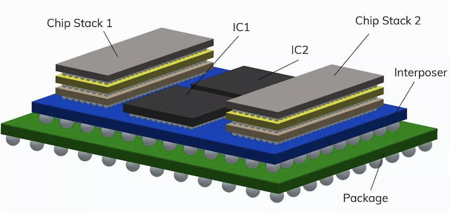
Modern semiconductor applications increasingly require advanced packaging solutions that extend beyond traditional wire-bond or flip-chip approaches:
System-in-Package (SiP) Integration
Heterogeneous Integration: Many applications benefit from combining different process technologies (RF, analog, digital, memory) in a single package. Foundry capabilities for heterogeneous integration, including die-to-die interconnect options and thermal management, become critical differentiators.
3D Integration Technologies: Through-silicon via (TSV) capabilities, wafer-level packaging, and die stacking technologies enable compact, high-performance solutions but require specialized foundry capabilities and qualification processes.
Embedded Technologies: Some applications benefit from embedded components (passive components, memory, MEMS devices) integrated directly into the package substrate or interposer, requiring foundry partnerships with advanced packaging providers.
Co-Design and Optimization Services
Package-Design Co-Optimization: Advanced applications require simultaneous optimization of die design and package characteristics to achieve optimal system performance. Foundries offering co-design services can provide significant advantages in time-to-market and performance optimization.
Thermal Simulation and Management: High-performance applications require sophisticated thermal modeling and management strategies. Foundry capabilities in thermal simulation, package design optimization, and thermal characterization can be critical success factors.
Signal Integrity Analysis: High-speed applications require comprehensive signal integrity analysis encompassing on-die interconnects, package routing, and system-level interactions. Foundry partnerships with electronic design automation (EDA) providers and package design houses can provide integrated solutions.
Quality Management and Process Control
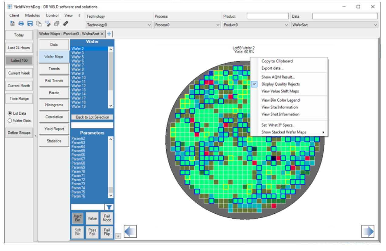
Statistical Process Control (SPC)
Foundry process control capabilities directly impact product quality and yield consistency:
Real-Time Monitoring Systems: Advanced foundries implement comprehensive SPC systems that monitor hundreds of process parameters in real-time, enabling rapid detection and correction of process excursions.
Predictive Maintenance Programs: Equipment reliability and consistency require predictive maintenance programs that prevent equipment-related defects and process variations. Understanding foundry maintenance practices provides insights into process stability expectations.
Continuous Improvement Culture: Long-term foundry partnerships benefit from continuous improvement cultures that systematically reduce defect rates and improve process capabilities over time.
Quality Certification and Compliance
Industry-Specific Certifications: Different applications require specific quality certifications (ISO 9001, AS9100 for aerospace, ISO/TS 16949 for automotive) that not all foundries maintain.
Audit and Compliance Verification: Critical applications may require regular quality audits and compliance verification processes. Understanding foundry audit policies and compliance support capabilities helps ensure long-term partnership viability.
Traceability and Documentation: Some applications require extensive lot traceability and documentation that may exceed standard foundry practices. Evaluating foundry capabilities for enhanced documentation and traceability helps ensure compliance with application-specific requirements.
Conclusion and Strategic Recommendations
The foundry selection process has evolved from a simple cost-performance trade-off to a complex strategic decision that impacts every aspect of semiconductor product development and lifecycle management. Success requires a systematic approach that considers technical capabilities, financial implications, supply chain risks, and long-term strategic alignment.
The framework presented in this guide provides a comprehensive methodology for evaluating foundry options across diverse application domains. However, the specific weighting and evaluation criteria must be tailored to individual project requirements, organizational capabilities, and strategic objectives.
As the semiconductor industry continues to evolve, foundry selection will become increasingly complex, with new technology options, changing geopolitical landscapes, and evolving customer requirements. Organizations that develop systematic foundry evaluation capabilities and maintain strategic foundry relationships will be best positioned to navigate this complexity and achieve sustainable competitive advantages.
The investment in comprehensive foundry evaluation processes pays dividends throughout the product lifecycle, from initial development through high-volume manufacturing and eventual product transitions. In an industry where foundry decisions can impact product success for years or decades, the importance of strategic foundry selection cannot be overstated.

![[STA] Synchronous Clocks vs. Asynchronous Clocks](https://images.unsplash.com/photo-1533749047139-189de3cf06d3?crop=entropy&cs=tinysrgb&fit=max&fm=jpg&ixid=M3wxMTc3M3wwfDF8c2VhcmNofDF8fGNsb2NrfGVufDB8fHx8MTc1NTQzMzg1OHww&ixlib=rb-4.1.0&q=80&w=600)

