US EDA Export Controls: A Strategic Analysis of Semiconductor Design Technology Restrictions and Their Global Impact

Executive Summary
The Trump administration's recent export control measures targeting Electronic Design Automation (EDA) software represent a paradigm shift in semiconductor geopolitics, fundamentally altering the landscape of global chip design capabilities. This comprehensive analysis examines the technical, economic, and strategic implications of restricting Synopsys, Cadence, and Siemens EDA technologies from Chinese markets, revealing critical vulnerabilities in the global semiconductor supply chain architecture.
The Technical Foundation: Understanding EDA's Critical Role in Modern VLSI Design
What Makes EDA Software Irreplaceable?
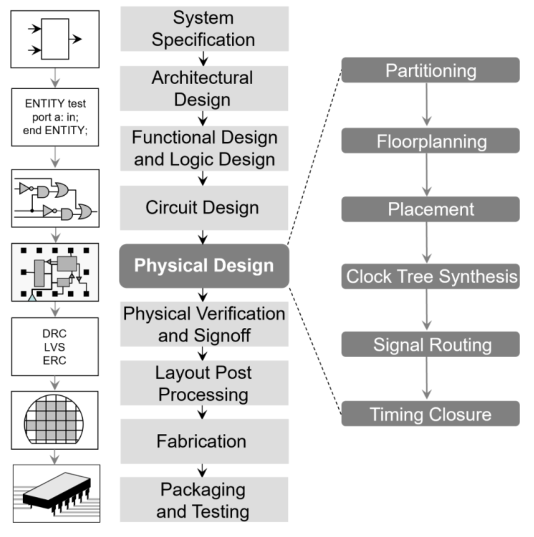
Electronic Design Automation represents the computational backbone of modern semiconductor design, encompassing a sophisticated ecosystem of tools that span from system-level architecture to physical implementation. The complexity of contemporary VLSI design—involving billions of transistors operating at sub-2nm process nodes—renders manual design approaches fundamentally obsolete.
Critical EDA Workflow Stages:
- System-Level Design & Architecture: High-level synthesis (HLS) tools that translate algorithmic descriptions into RTL implementations
- Logic Synthesis: Converting RTL descriptions into gate-level netlists optimized for area, power, and timing
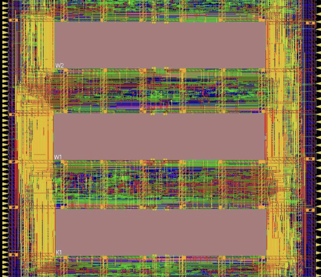
- Physical Design & Place-and-Route: Automated placement and routing algorithms handling billions of interconnects
- Design for Manufacturability (DFM): Advanced lithographic modeling and resolution enhancement techniques
- Verification & Validation: Formal verification, simulation, and sign-off analysis ensuring design correctness
The Oligopoly's Technical Dominance
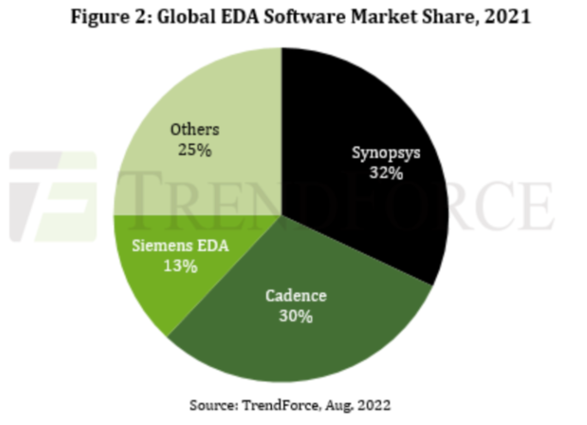
The EDA industry's market concentration reflects not merely economic dynamics but fundamental technical barriers to entry. Synopsys and Cadence collectively command 62% market share, but this understates their dominance in critical subsegments:
Logic Synthesis Tools:
- Synopsys Design Compiler: most of market share in logic synthesis
- Cadence Genus: Primary competitor with advanced machine learning optimization
Physical Design:
- Synopsys IC Compiler II: Leading-edge place-and-route for advanced nodes
- Fusion compiler: Synopsys' new-generation product with synthesis and P&R
- Cadence Innovus: Competitive solution with superior congestion handling
- The traditional number 1 is Synopsys, but many customers are switching to Innovus.
- I have used Synopsys & Cadence products, and I personally feel that the Cadence tool is easy for beginners, while Synopsys products are the best for experienced users.
- More discussions:

How different are Cadence Innovus and Synopsys ICC2?
by u/greenndreams in chipdesign
Which Synopsys or Cadence Software for RTL to GDSII
by u/metalzero24 in chipdesign
Is Synopsys more user friendly to beginners compared to Cadence?
by u/DragonicStar in chipdesign
Verification Platforms:
- Synopsys VCS: Industry standard for simulation and verification
- Cadence Xcelium: Advanced parallel simulation technology
Critical Insight: While overall market share appears competitive, specific tool categories exhibit near-monopolistic concentration. For instance, Synopsys dominates static timing analysis (PrimeTime) and power analysis (PrimePower) with >80% market share in advanced node designs.
I have not heard of a single Mask Tape Out (MTO) with Cadence Tempus in Korea in the last 6 months.
Considering that Big companies usually take 2 years to design semiconductors for mass production(MP) and spend $30M or more for even relatively simple chips, they want a proven EDA tool. That is PrimeTime.
Geopolitical Context: The Strategic Chess Game
Beyond Trade Wars: Technology Sovereignty
The EDA export restrictions represent a sophisticated understanding of technological dependency structures. Unlike previous export controls targeting manufacturing equipment or finished products, these measures target the intellectual foundation of semiconductor design itself.
Strategic Rationale Analysis:
- Chokepoint Control: EDA tools represent a critical bottleneck where three companies control global design capabilities
- Innovation Throttling: Advanced node design requires cutting-edge EDA capabilities unavailable elsewhere
- Ecosystem Lock-in: EDA tools create deep technical dependencies through proprietary formats and methodologies
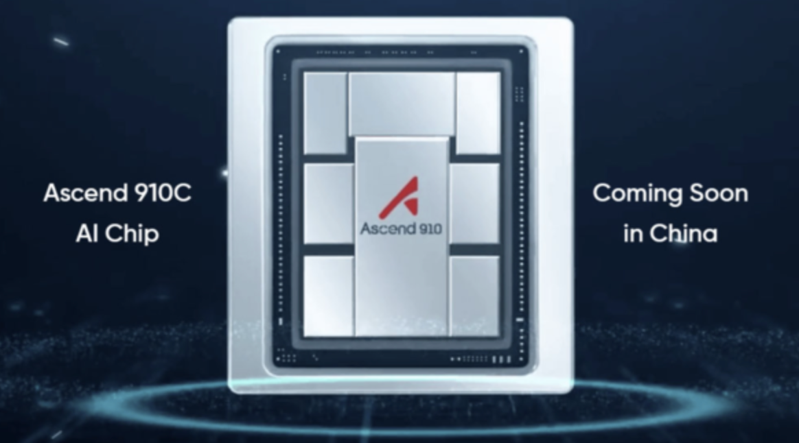
The Huawei Precedent and Escalation Dynamics
The January 13th expansion of Huawei restrictions to global usage of Ascend chips demonstrates the administration's willingness to leverage extraterritorial jurisdiction. This creates a compliance dilemma for global semiconductor companies, forcing binary choices between Chinese and Western markets.
Technical Impact Assessment: Quantifying the Damage
Immediate Consequences for Chinese Semiconductor Design
Advanced Node Design Capabilities: Chinese fabless companies designing at 7nm and below face immediate critical challenges:
- Synthesis Optimization: Legacy tools cannot achieve the required power-performance-area (PPA) targets
- Physical Implementation: Sub-7nm place-and-route requires advanced congestion prediction algorithms unavailable in Chinese tools
- DFM Compliance: TSMC and Samsung's advanced processes require specific EDA tool certification
Quantitative Impact Metrics:
- Design productivity degradation: 40-60% for advanced node projects
- Time-to-market delays: 6-18 months for complex SoCs
- Design quality degradation: 15-25% PPA penalty using alternative tools
License Management: The Hidden Vulnerability
The analysis correctly identifies license dependency as a critical control mechanism. Modern EDA licenses employ sophisticated authentication systems:
Technical Architecture:
- Cloud-based license servers with encrypted authentication
- Hardware fingerprinting preventing license portability
- Automatic update mechanisms for tool enhancement
Control Mechanism Effectiveness: Even pre-purchased licenses become obsolete without:
- Bug fixes and patches critical for design closure
- Process design kit (PDK) updates for new foundry processes
- Performance optimization updates essential for competitive designs
Chinese EDA Ecosystem: Current Capabilities and Limitations
Domestic Tool Assessment
Strengths in Specific Segments:
- Analog Design: Primarius (empyrean) provides competitive mixed-signal design tools
- PCB Design: Altium-equivalent capabilities from multiple vendors
- System-Level Design: Reasonable capabilities in architectural exploration
Critical Gaps in Advanced Digital Design:
- Logic Synthesis: 2-3 technology generations behind in optimization algorithms
- Physical Implementation: Limited scalability for designs >100M gates
- Sign-off Analysis: Inadequate correlation with foundry characterization
The Engineer Paradox
The observation about Chinese-American engineers in US EDA companies reveals a fascinating irony. Approximately 30-40% of senior EDA engineers at major US companies are of Chinese origin, creating complex knowledge transfer dynamics that export controls cannot easily address.
Strategic Response Scenarios and Long-term Implications
Scenario 1: Accelerated Indigenous Development
Probability: High (60-70%)
China's response likely involves massive state investment in EDA development, potentially leveraging:
- Returning overseas talent with deep EDA expertise
- University-industry collaboration programs
- Open-source EDA initiatives (OpenROAD, OpenLane extensions)
Timeline Estimate: 5-7 years for competitive advanced node tools
Scenario 2: Alternative Ecosystem Development
Probability: Medium (30-40%)
Development of China-centric design methodologies optimizing for domestic foundry capabilities rather than matching Western tool functionality.
Scenario 3: Circumvention Through Third Countries
Probability: Low (10-20%)
Technical complexity and license tracking make circumvention difficult, though possible through academic institutions or joint ventures.
Market Dynamics and Economic Impact
Revenue Implications for EDA Vendors
China represents approximately 15-20% of global EDA revenue (~$2.5-3B annually). However, growth projections suggested Chinese market expansion to $1B+ by 2025, representing significant future revenue loss.
Foundry Ecosystem Disruption
Taiwan and Korean foundries face complex compliance challenges, potentially losing Chinese fabless customers while maintaining US tool vendor relationships.
Recommendations and Strategic Outlook
For Global Semiconductor Companies
- Diversify EDA Tool Dependencies: Develop multi-vendor strategies reducing single-point-of-failure risks
- Invest in Internal Capabilities: Build proprietary design flows for competitive differentiation
- Monitor Compliance Requirements: Establish robust export control compliance programs
For the EDA Industry
- Innovation Acceleration: Leverage current market position to advance technological leadership
- Partnership Strategies: Develop alliance structures maintaining market access while ensuring compliance
- Talent Retention: Address potential brain drain as geopolitical tensions affect engineer mobility
For Policymakers
- Coalition Building: Coordinate with allied nations to prevent circumvention through alternative suppliers
- Innovation Investment: Support domestic EDA ecosystem development through targeted R&D funding
- Long-term Strategy: Develop comprehensive approach addressing both offensive and defensive technology protection
Conclusion: The New Reality of Semiconductor Geopolitics
The EDA export controls represent a sophisticated understanding of technological dependency structures, targeting the intellectual foundation of semiconductor advancement rather than manufacturing capabilities alone. While short-term impacts favor US strategic objectives, long-term consequences may accelerate Chinese indigenous development and fragment global technology ecosystems.
The semiconductor industry enters an era where geopolitical considerations increasingly override pure economic optimization, fundamentally altering competitive dynamics and innovation patterns. Success in this environment requires not only technical excellence but also sophisticated understanding of regulatory landscapes and supply chain vulnerabilities.
As the technology cold war intensifies, EDA tools emerge as both weapons and shields in the battle for semiconductor supremacy, with implications extending far beyond the immediate US-China rivalry to reshape global technology architecture for decades to come.

![[STA] Synchronous Clocks vs. Asynchronous Clocks](https://images.unsplash.com/photo-1533749047139-189de3cf06d3?crop=entropy&cs=tinysrgb&fit=max&fm=jpg&ixid=M3wxMTc3M3wwfDF8c2VhcmNofDF8fGNsb2NrfGVufDB8fHx8MTc1NTQzMzg1OHww&ixlib=rb-4.1.0&q=80&w=600)

