What is a Semiconductor?: Technical Interview Question Guide

Imagine you're in the final interview at your dream company and they ask: "What is a semiconductor? Please explain in detail"
1. Band Theory Explanation
A semiconductor is a solid material with electrical conductivity between that of a conductor (metal) and an insulator. From a band structure perspective, semiconductors are characterized by an energy gap (band gap) of approximately 0.5-3 eV between the conduction band and valence band.

reference: https://www.geeksforgeeks.org/fermi-energy/
At absolute zero (0K), semiconductors behave like insulators with a completely filled valence band and empty conduction band. However, at room temperature, the band gap is small enough that thermal energy can excite some carriers (electrons or holes) to higher energy states.
Key Process: Electrons excited to the conduction band and the holes left behind in the valence band both contribute to electrical conduction.
Summary: While semiconductors don't conduct electricity as well as metals, their conductivity can be easily controlled through external energy or doping, which dramatically changes the carrier concentration.
Generally, semiconductors are materials that have a small band gap at room temperature with the Fermi level positioned within the band gap region.
2. Intrinsic vs. Extrinsic Semiconductors
2.1 Intrinsic Semiconductors
Intrinsic semiconductors are pure semiconductors without impurities. In a silicon crystal, when an electron is excited to the conduction band, a hole is created in the valence band in a 1:1 ratio.
At equilibrium, the electron concentration (n) equals the hole concentration (p), known as the intrinsic carrier concentration. This intrinsic carrier concentration is very small at room temperature.
Pure silicon has low conductivity (resistivity ~10⁵ Ω·cm) due to the minimal number of free electrons and holes.
2.2 Extrinsic Semiconductors
To achieve higher conductivity, small amounts of impurities are added through doping to create extrinsic semiconductors. Doping significantly alters either electron or hole concentrations.
n-type Doping:
- Adding pentavalent donor atoms (P, As, Sb) to silicon (tetravalent)
- Donors easily ionize, providing electrons to the conduction band
- Electrons become majority carriers
- Fermi level shifts upward toward the conduction band
p-type Doping:
- Adding trivalent acceptor atoms (B, Al) creates electron deficiency
- Acceptors capture electrons from neighboring atoms, leaving holes
- Holes become majority carriers
- Fermi level shifts downward toward the valence band
At room temperature, impurities are typically fully ionized, so the majority carrier concentration approximates the doping concentration, resulting in significantly improved conductivity compared to intrinsic semiconductors.
Industrial Context: Commercial semiconductors are typically extrinsic semiconductors with completed doping.
3. Temperature Effects on Semiconductors
Temperature changes significantly affect carrier concentration and mobility in semiconductors.
Intrinsic Excitation: In pure semiconductors, increasing temperature dramatically increases thermal excitation, promoting more electrons to the conduction band and creating more holes.
Freeze-Out: At low temperatures, even doped semiconductors experience insufficient ionization of donors or acceptors, causing most free carriers to disappear.
Extrinsic Range: In intermediate temperature ranges, donors and acceptors are fully ionized, making majority carrier density approximately equal to the doping concentration. While carrier count remains relatively constant with temperature, lattice vibrations (phonons) increase, reducing mobility and slightly decreasing conductivity.
Intrinsic Takeover: At higher temperatures, intrinsic carriers exceed the doping concentration. The semiconductor essentially behaves intrinsically, with conductivity increasing sharply with temperature. This causes the rapid increase in leakage current at high temperatures.
Commercial Standard: Semiconductor operating conditions are typically designed for -40°C to 125°C.

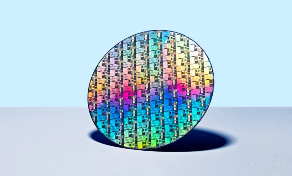
4. Why Silicon Became the Dominant Semiconductor Material
Crystal Structure & Purity
- Silicon crystallizes in a diamond cubic structure
- Large-diameter, high-purity single crystals can be grown using processes like Czochralski
- Wide-area wafers are more easily obtainable compared to other elements
- Silicon is abundant in Earth's crust, making it cost-effective
Band Gap & Electrical Properties
- Silicon has an indirect band gap of ~1.12 eV (at 300K)
- Intrinsic carrier concentration is ~10¹⁰ cm⁻³ at room temperature
- Electron mobility: ~1400 cm²/V·s
- Hole mobility: ~600 cm²/V·s
- These properties are sufficient for most logic device implementations
SiO₂ Formation
- High-temperature oxidation of silicon forms silicon dioxide (SiO₂)
- SiO₂ has excellent insulating properties with minimal semiconductor-oxide interface defects
- Stable oxidation process with minimal degradation maintains high yield
- This became fundamental for MOS structure development and high-density integration
- Other semiconductors (like GaAs) cannot form such high-quality oxide layers cost-effectively
Process Maturity
- Decades of silicon process technology development
- Extensive infrastructure for doping, oxidation, lithography, etching, and deposition
- Good mechanical strength and thermal conductivity for high-temperature processing
Bottom Line: Silicon's combination of affordability, appropriate band gap, good mobility, and process advantages made it the industry standard.
5. Compound Semiconductors and Specialized Applications
Compound semiconductors consist of two or more elements and serve specialized roles that silicon cannot effectively perform.
Gallium Arsenide (GaAs)
- Band gap: ~1.42 eV
- High luminous efficiency for LEDs and lasers
- Higher electron mobility than silicon for RF applications
- Limited by substrate growth challenges, oxide formation difficulties, and mechanical strength compared to silicon
Silicon Carbide (SiC)
- Band gap: ~3.26 eV (4H-SiC)
- High breakdown field (~2-3×10⁶ V/cm)
- Excellent thermal conductivity
- Ideal for high-voltage, high-temperature, high-power devices
- Applications: EV drive MOSFETs, IGBTs, Schottky diodes
Gallium Nitride (GaN)
- Band gap: 3.4 eV
- Excellent electron mobility (especially in AlGaN/GaN heterostructures with 2D electron gas)
- High-frequency, high-power HEMT applications
- Blue/UV wavelength LEDs and laser diodes
Other Compound Semiconductors
- Indium Phosphide (InP), GaSb, CdTe, ZnSe
- Used in optical communications, sensors, and solar cells
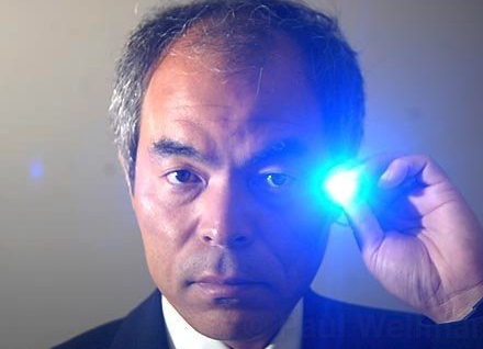
Historical Note: Shuji Nakamura received the Nobel Prize for developing blue LEDs using compound semiconductors.
6. P-N Junctions: The Foundation of Modern Electronics
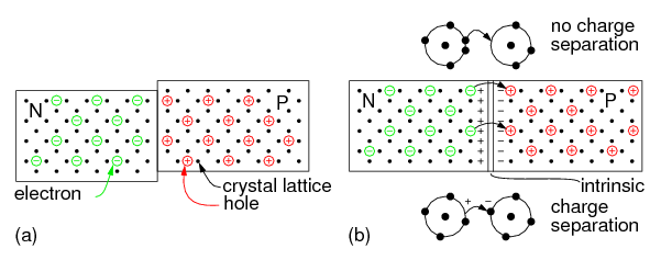
When p-type and n-type semiconductors are brought together, they form a p-n junction—the fundamental building block of virtually all semiconductor devices. The behavior of this junction under different bias conditions enables the creation of diverse electronic and optoelectronic devices.
6.1 P-N Junction Physics
Formation and Equilibrium: When p-type and n-type materials are joined, majority carriers diffuse across the junction due to concentration gradients. Electrons from the n-side diffuse to the p-side, while holes from the p-side diffuse to the n-side. This creates a space charge region (depletion region) where mobile carriers are depleted, leaving behind ionized dopant atoms.
Built-in Potential: The charge separation creates an electric field that opposes further diffusion, establishing equilibrium with a built-in potential (Vbi) given by:
Vbi = (kT/q) × ln(NaNd/ni²)where Na and Nd are acceptor and donor concentrations, respectively, and ni is the intrinsic carrier concentration.
Depletion Width: The depletion region width (W) depends on the built-in potential and doping levels:
W = √(2εs(Na + Nd)Vbi/q(NaNd))6.2 Bias Conditions and I-V Characteristics
Forward Bias (p-side positive, n-side negative):
- Reduces the electric field across the junction
- Lowers the potential barrier for majority carrier injection
- Exponential current increase described by the Shockley equation:
I = Is(e^(qV/nkT) - 1)where Is is the saturation current and n is the ideality factor.
Reverse Bias (p-side negative, n-side positive):
- Increases the electric field and widens the depletion region
- Majority carriers are swept away from the junction
- Only small reverse saturation current flows due to minority carriers
- Junction capacitance decreases with increasing reverse bias
https://www.allaboutcircuits.com/textbook/semiconductors/chpt-2/the-p-n-junction/
7. Semiconductor Devices and Applications
7.1 Bipolar Junction Transistors (BJTs)
Structure: Three-layer devices (npn or pnp) with two p-n junctions
- Emitter-Base Junction: Forward biased in active mode
- Base-Collector Junction: Reverse biased in active mode
Operation Principle: In an npn transistor, electrons injected from the emitter into the base are collected by the collector. The base current controls the collector current through current gain (β):
IC = β × IBApplications: Amplifiers, switches, and analog circuits where high current gain and low noise are required.
7.2 Field-Effect Transistors (FETs)
MOSFET Structure: Metal-Oxide-Semiconductor structure with gate, source, and drain
- Gate Oxide: Provides electrical isolation between gate and channel
- Channel Formation: Gate voltage modulates channel conductivity
Operation Modes:
- Enhancement Mode: Channel forms when gate voltage exceeds threshold voltage (Vth)
- Depletion Mode: Existing channel is modulated by gate voltage
Key Equations:
- Linear Region: ID = μnCox(W/L)[(VGS - Vth)VDS - VDS²/2]
- Saturation Region: ID = (μnCox/2)(W/L)(VGS - Vth)²
Advantages: High input impedance, low power consumption, excellent scalability for digital circuits.
7.3 Photodetectors
Operating Principle: Reverse-biased p-n junctions where incident photons generate electron-hole pairs
- Photocurrent: Proportional to incident optical power
- Spectral Response: Determined by band gap and absorption coefficient
- Quantum Efficiency: η = (Number of collected carriers)/(Number of incident photons)
Types:
- PIN Photodiodes: Intrinsic region between p and n regions for enhanced sensitivity
- Avalanche Photodiodes (APDs): Internal gain through impact ionization
- Phototransistors: Optical input controls base current
Applications: Optical communications, imaging systems, light detection and ranging (LiDAR).
7.4 Solar Cells (Photovoltaic Devices)
Energy Conversion Mechanism: Photons with energy ≥ band gap create electron-hole pairs
- Open-Circuit Voltage (Voc): Maximum voltage under illumination
- Short-Circuit Current (Isc): Maximum current under illumination
- Fill Factor (FF): Ratio of maximum power to Voc × Isc
Efficiency Limitations:
- Shockley-Queisser Limit: Theoretical maximum efficiency (~33% for single junction)
- Thermalization Losses: Excess photon energy converted to heat
- Transmission Losses: Sub-bandgap photons not absorbed
Advanced Architectures:
- Tandem Cells: Multiple junctions with different band gaps
- Concentrator Systems: Optical concentration to increase efficiency
- Perovskite-Silicon Tandems: Emerging high-efficiency technology
7.5 Light-Emitting Diodes (LEDs)
Electroluminescence Process: Forward-biased p-n junction where recombining electron-hole pairs emit photons
- Emission Wavelength: λ = hc/Eg (where Eg is the band gap)
- External Quantum Efficiency: ηext = ηint × ηextraction
Material Systems:
- Red/IR: AlGaAs, GaAsP
- Green/Yellow: AlGaInP, GaN
- Blue/UV: InGaN/GaN quantum wells
- White Light: Blue LED + phosphor or RGB combination
Advanced Structures:
- Quantum Wells: Carrier confinement for improved efficiency
- Distributed Bragg Reflectors: Enhanced light extraction
- Micro-LEDs: Miniaturized devices for display applications
7.6 Laser Diodes
Stimulated Emission: Population inversion in the active region enables coherent light emission
- Threshold Current: Minimum current for lasing action
- Optical Cavity: Fabry-Perot or distributed feedback (DFB) structures
- Mode Control: Single-mode operation for communications
Key Parameters:
- Differential Efficiency: Slope of L-I curve above threshold
- Linewidth Enhancement Factor: Coupling between amplitude and phase modulation
- Relative Intensity Noise (RIN): Spectral density of intensity fluctuations
Applications: Optical communications, laser processing, spectroscopy, LiDAR.
8. Advanced Device Physics and Emerging Technologies
8.1 Quantum Effects in Nanoscale Devices
Quantum Confinement: When device dimensions approach the de Broglie wavelength, quantum effects become significant
- Quantum Wells: 1D confinement affects density of states
- Quantum Wires: 2D confinement creates 1D electronic systems
- Quantum Dots: 3D confinement leads to discrete energy levels
Tunneling Phenomena:
- Tunnel Diodes: Negative differential resistance from band-to-band tunneling
- Resonant Tunneling Diodes: Quantum well structures with resonant states
- Tunnel FETs: Steep subthreshold slope through tunneling injection
8.2 High-Electron-Mobility Transistors (HEMTs)
Heterostructure Engineering: Different band gap materials create 2D electron gas (2DEG)
- AlGaN/GaN HEMTs: High power density for RF applications
- AlGaAs/GaAs HEMTs: Low noise for microwave circuits
- InAlAs/InGaAs HEMTs: Ultra-high frequency performance
Performance Metrics:
- Cutoff Frequency (fT): Unity current gain frequency
- Maximum Oscillation Frequency (fmax): Unity power gain frequency
- Power Added Efficiency (PAE): (Pout - Pin)/PDC
8.3 Power Electronics Devices
Wide Bandgap Semiconductors: SiC and GaN enable high-voltage, high-temperature operation
- SiC MOSFETs: Automotive traction inverters, industrial motor drives
- GaN HEMTs: Power adapters, wireless charging, data center power supplies
- SiC Schottky Diodes: Fast switching with minimal reverse recovery
Figure of Merit: Baliga's Figure of Merit (BFOM) = εμE³c quantifies material performance for power switching.
8.4 Emerging Device Concepts
Negative Capacitance Transistors: Ferroelectric materials provide voltage amplification Spin-Based Devices: Magnetic tunnel junctions for non-volatile memory Neuromorphic Devices: Memristors and synaptic transistors for brain-inspired computing Topological Insulators: Edge states for quantum computing applications
9. Device Fabrication and Integration Challenges
9.1 Scaling Limitations
- Short Channel Effects: Threshold voltage roll-off, drain-induced barrier lowering
- Quantum Tunneling: Gate leakage through ultra-thin oxides
- Variability: Statistical dopant fluctuations, line edge roughness
9.2 Advanced Process Technologies
- FinFET Architecture: 3D channel control for improved electrostatics
- Gate-All-Around (GAA): Nanowire/nanosheet devices for ultimate scaling
- Monolithic 3D Integration: Vertical stacking of active devices
9.3 Heterogeneous Integration
- System-in-Package (SiP): Combining different semiconductor technologies
- Chiplet Architecture: Disaggregated design with advanced packaging
- Photonic Integration: Co-integration of electronics and photonics
Conclusion: The p-n junction serves as the fundamental building block that enables an extraordinary diversity of semiconductor devices. From simple diodes to complex quantum devices, the ability to control carrier transport through junction engineering and bias conditions has revolutionized modern technology

![[STA] Synchronous Clocks vs. Asynchronous Clocks](https://images.unsplash.com/photo-1533749047139-189de3cf06d3?crop=entropy&cs=tinysrgb&fit=max&fm=jpg&ixid=M3wxMTc3M3wwfDF8c2VhcmNofDF8fGNsb2NrfGVufDB8fHx8MTc1NTQzMzg1OHww&ixlib=rb-4.1.0&q=80&w=600)

