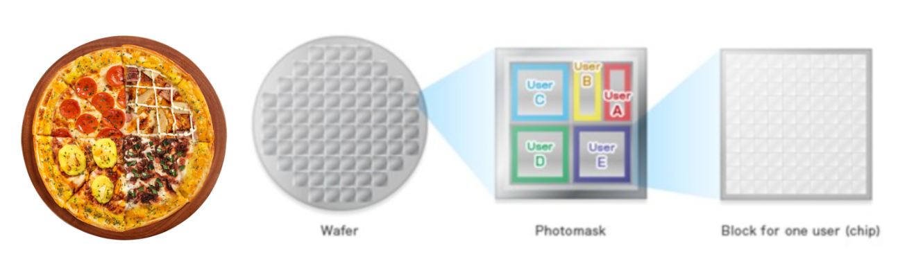
What is MPW (Multi-Project Wafer)?


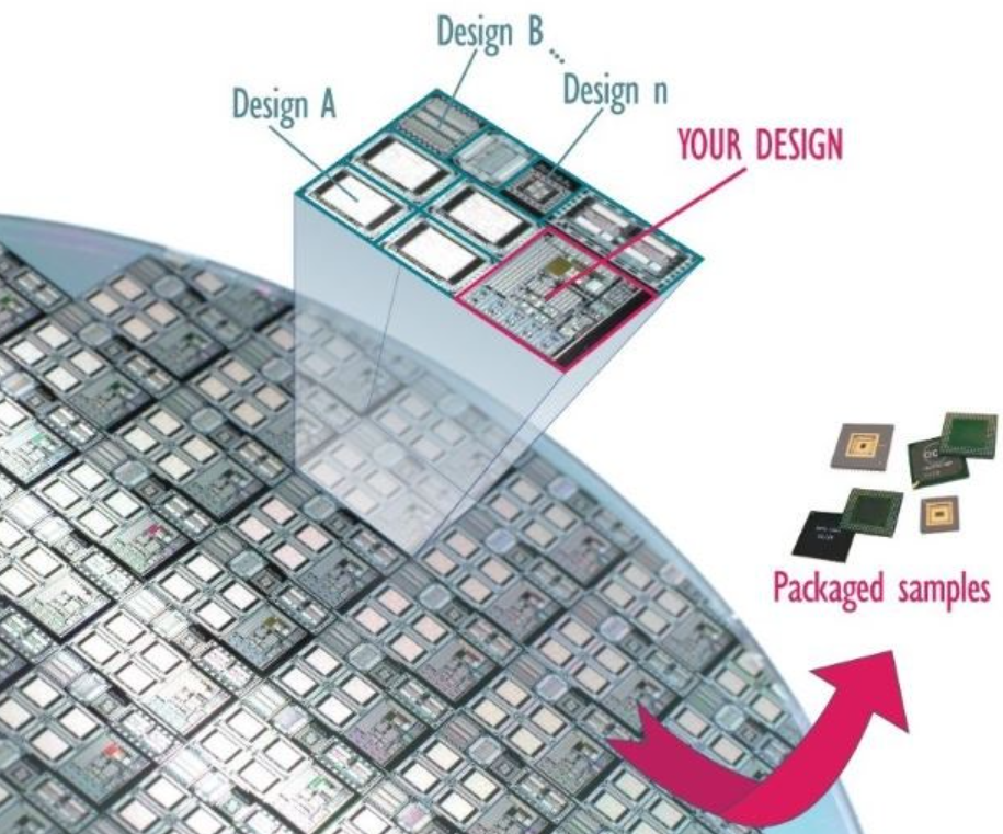
Multi-Project Wafer (MPW) is a service that allows various semiconductor designs to be fabricated on a single wafer.
Think of it like a "variety pizza"—instead of ordering a full pizza with just one topping, an MPW wafer combines multiple different designs from various teams onto a single wafer.
Why MPW?
Because designing and manufacturing semiconductors is incredibly expensive.
For a single cutting-edge wafer, the cost can range from tens of millions to over a hundred million USD. MPW allows different companies to share the cost of one wafer, making it a highly cost-effective way to produce initial prototypes.
The Strategic Value of MPW
1. Cost-Effectiveness
By grouping multiple IC designs onto a single maskset, MPW can reduce prototyping costs by up to 90%.
This dramatically lowers Non-Recurring Engineering (NRE) costs, which are a major financial barrier for small companies and startups.
The cost of the mask is shared, making it accessible for projects that couldn't otherwise afford a dedicated production run.
2. Shorter Time-to-Market
MPW services offer a rapid feedback loop for validating designs and intellectual property (IP).
This allows teams to quickly test and debug their concepts on real silicon, accelerating the development process and getting products to market faster.
3. Risk Mitigation
As process nodes get smaller and maskset costs skyrocket, the risk of a design error requiring a costly respin (re-fabrication) is financially devastating.
MPW allows designers to perform essential adjustments on a smaller, cheaper run, significantly reducing the financial risk associated with full-scale production.
4. Accessibility
MPW lowers the barrier to entry for startups, researchers, and small businesses, democratizing access to cutting-edge manufacturing technology.
This is especially important for exploring new fields like IoT, AI, and 5G, where customized chips are in high demand.
The Future of MPW
The semiconductor industry is an incredibly challenging space for startups due to the high costs and complexity. The initial rounds of funding are particularly difficult, as manufacturing costs are a significant hurdle.
If MPW costs remain high, it could limit the number of innovative ideas that can be prototyped. To foster a vibrant ecosystem, it's essential to not only have a well-integrated network of foundries, EDA, and IP providers but also a strong investment ecosystem involving venture capital and government support.
MPW has the potential to democratize silicon innovation, making it a critical catalyst for the industry's future.

![[STA] Synchronous Clocks vs. Asynchronous Clocks](https://images.unsplash.com/photo-1533749047139-189de3cf06d3?crop=entropy&cs=tinysrgb&fit=max&fm=jpg&ixid=M3wxMTc3M3wwfDF8c2VhcmNofDF8fGNsb2NrfGVufDB8fHx8MTc1NTQzMzg1OHww&ixlib=rb-4.1.0&q=80&w=600)

