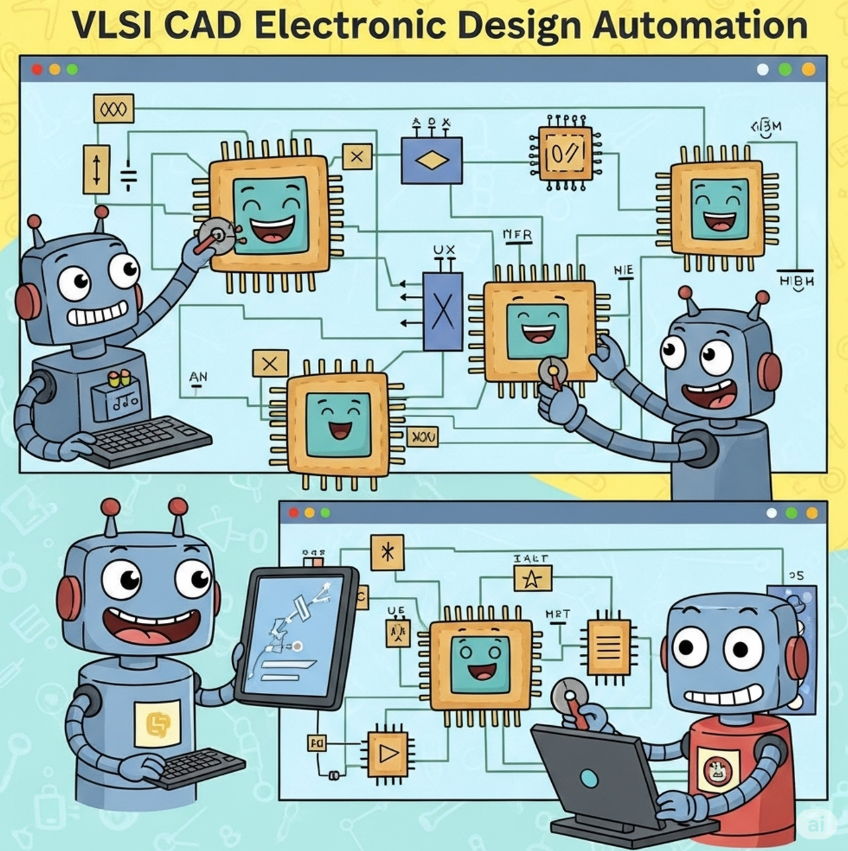
What is VLSI CAD and EDA?: Electronic Design Automation

All electronic devices that underpin modern society—smartphones, computers, automobiles, AI servers, and more—cannot exist without semiconductor chips.

These tiny chips integrate billions of microscopic transistors onto a single piece of silicon, a highly integrated technology known as Very Large Scale Integration (VLSI).
VLSI is not merely a continuation of technological progress; it represents a revolutionary approach to managing unprecedented levels of complexity. Efficiently designing and implementing complex systems with countless interacting components is a core challenge of the modern electronics industry.
The process of designing and verifying such complex chips is impossible with human capabilities alone. This is where EDA (Electronic Design Automation) comes into play.
EDA refers to the use of computer-aided design (CAD) software to automate the functional design, synthesis, verification, and physical design (including layout and wiring) of VLSI chips. It encompasses a broad category including hardware, software, services, and processes, serving as an essential tool to overcome the limitations of manual design, minimize bugs and defects, and enable rapid development.
EDA is not just a tool for efficiency; it is the very reason for the existence of the modern electronics industry and a fundamental technology that enables innovation. Managing billions of circuit elements manually is impossible, and without EDA, designing and manufacturing today's semiconductor devices would be unfeasible.

As the complexity of semiconductor chips increases exponentially, the difficulty of design and verification also rises proportionally. In this context, EDA plays a crucial role in shortening design cycles (time-to-market), reducing costs, and improving product quality and reliability.
EDA goes beyond mere cost reduction; it acts as a key driver for innovation speed and market competitiveness. Faster development and reduced errors lead directly to quicker market entry, and design errors requiring a re-spin can cost millions of dollars and several months.
Therefore, pre-verification through EDA directly translates to immense cost savings. Ultimately, EDA is a strategic business imperative that helps companies produce chips of the right quality at the right time to gain market advantage.
History of Semiconductor Design:
Limitations of the Manual Design Era

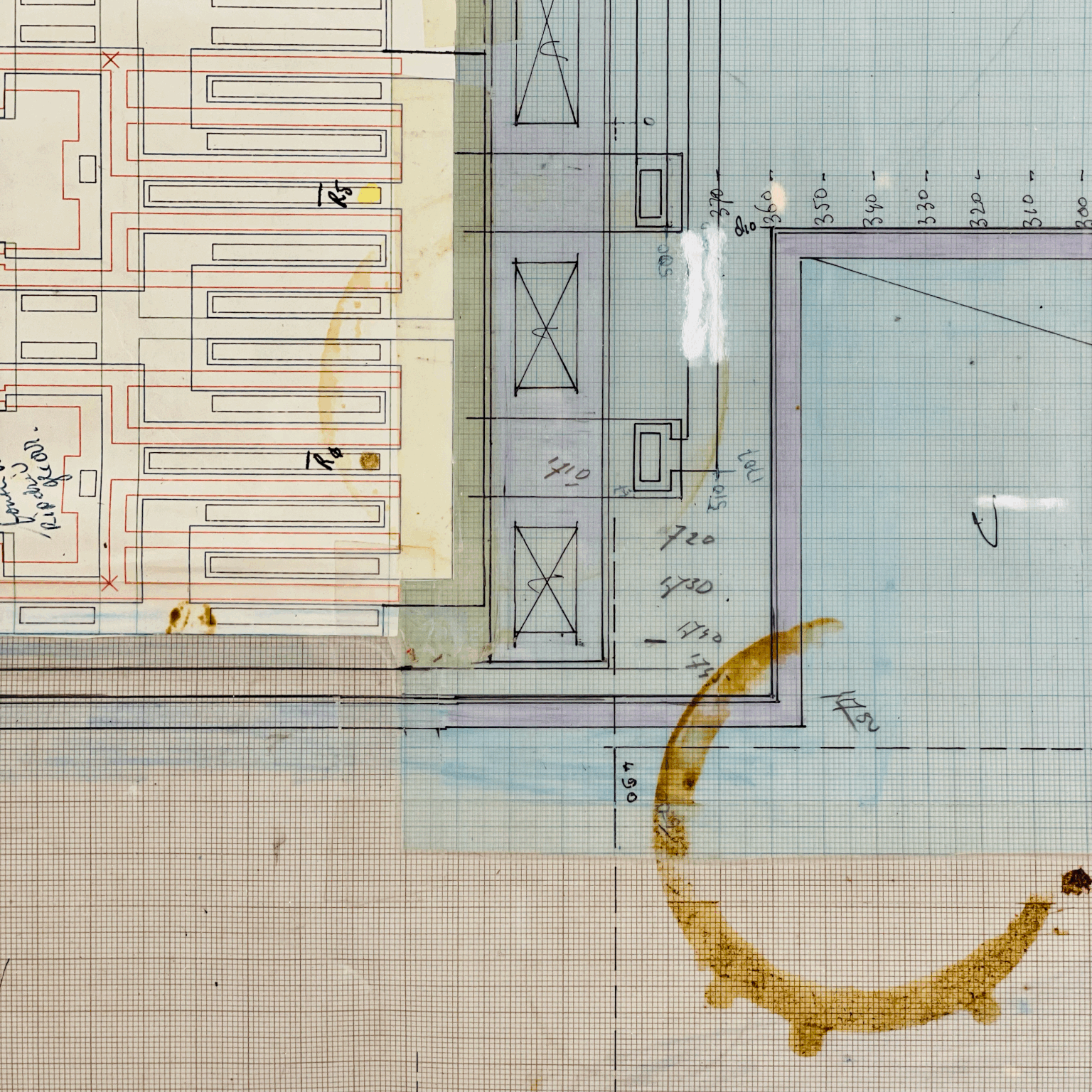
Before the advent of electronic design automation, the design and wiring of integrated circuits were entirely manual. At that time, circuits were far less complex than they are today, making such manual work feasible.
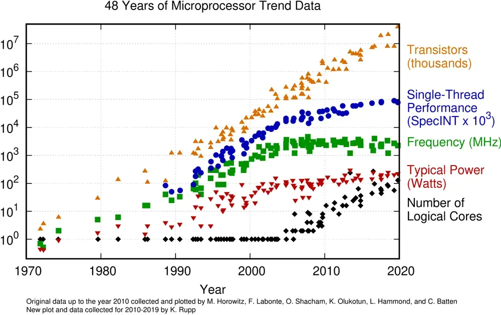
However, as the number of transistors increased exponentially (a phenomenon predicted by Moore's Law), the limitations of manual design became clear. It became impossible for human cognitive abilities alone to manage billions of elements and their subtle interactions, or to identify errors.
Furthermore, the time required for manual layout and verification made product development cycles unacceptably long.
These limitations were not merely inefficiencies but stemmed from fundamental human cognitive and time constraints. This marked a transition in semiconductor design from a craft-like, labor-intensive process to an engineering discipline reliant on computing power.
And there was no way to avoid coffee stains like the one below.😀
The Birth and Innovation of EDA: The Mead-Conway Revolution
From the mid-1970s, the semiconductor industry began attempts to automate the entire design process, moving beyond just mask sketch automation. A significant turning point in these efforts was the paper "Introduction to VLSI Systems," published by Carver Mead and Lynn Conway in 1980.
This seminal paper introduced new ideas for chip design through programming languages, a fundamentally different approach from previous geometric design methods.

The Mead-Conway revolution was a fundamental shift that transformed hardware design into a software development paradigm. Programming languages (e.g., Hardware Description Languages, HDL) enabled the abstract, text-based description of hardware behavior and structure. This is analogous to how high-level programming languages abstract away machine-level details in software development. Such abstraction plays a key role in managing complexity, enabling modularity and reusability. This change made chip design more scalable, reduced the likelihood of errors, and broadened accessibility to a wider range of engineers who could think in terms of logic and algorithms rather than physical geometry. This laid the intellectual foundation for modern digital design flows and the entire EDA industry.
ABEL: The First HDL
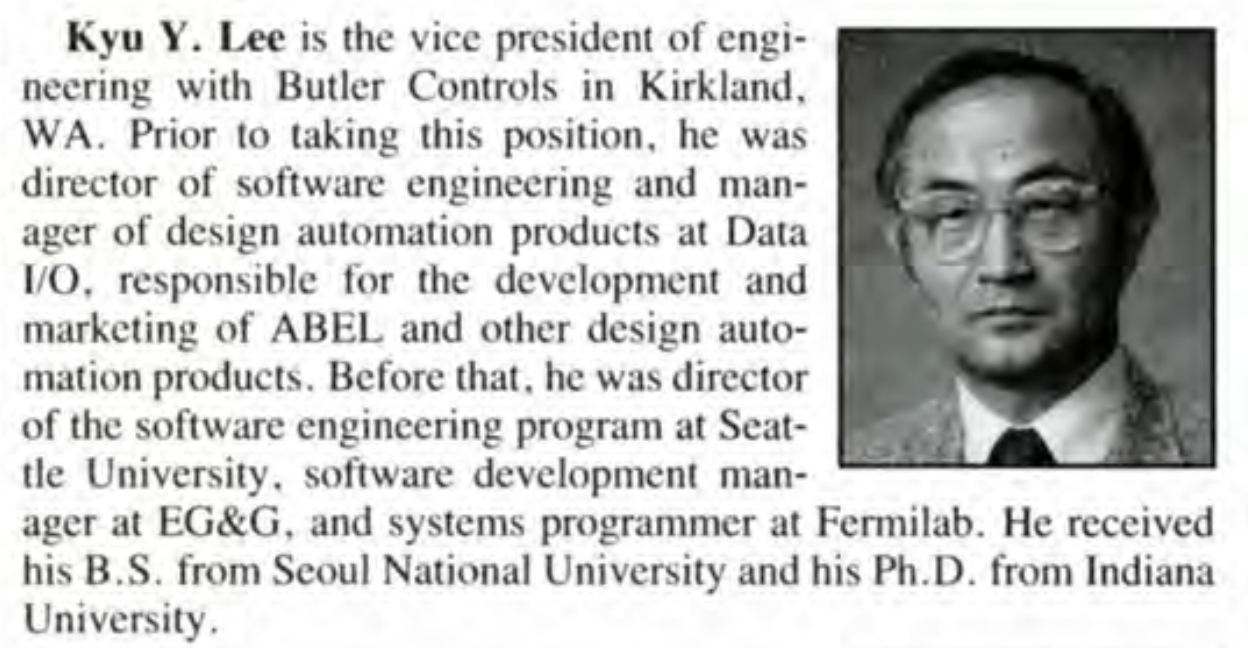
The Advanced Boolean Expression Language (ABEL) is widely regarded as one of the earliest HDLs, developed in 1983 by Data I/O Corporation in Redmond, Washington.
The concept and original compiler were created by Russell de Pina in 1981, with further development led by Dr. Kyu Y. Lee.
ABEL was designed to program Programmable Logic Devices (PLDs), offering formats like concurrent equations, truth tables, and sequential state machines. It also supported test vectors for verifying circuit behavior.
ABEL’s preprocessor used syntax inspired by Digital Equipment Corporation’s MACRO-11 assembly language. Contemporary languages like CUPL and PALASM served similar purposes, but ABEL’s simplicity made it popular in the 1980s.
However, with the rise of Field-Programmable Gate Arrays (FPGAs), ABEL’s usage declined.
Verilog: The Hardware Modeling Language
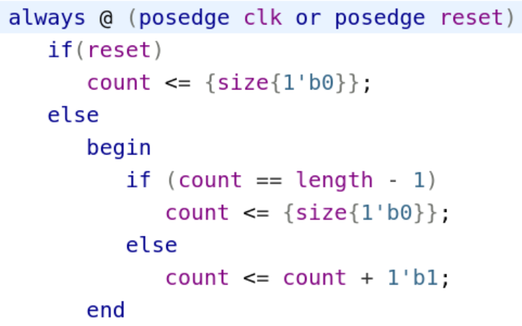
Introduced in 1984 by Automated Integrated Design Systems (later acquired by Cadence Design Systems), Verilog was initially developed as a hardware modeling language, making it particularly suited for verification tasks.
Its syntax, resembling the C programming language, allows for concise code, which appeals to engineers transitioning from software development. Verilog supports two main data types: net data types (e.g., wire) for connecting components and variable data types (e.g., reg) for temporary storage. Its ease of use and flexibility have made it a standard in the private sector for designing Application-Specific Integrated Circuits (ASICs) and FPGAs.
Verilog’s less rigid type system compared to VHDL allows for faster prototyping but may lead to errors if not carefully managed.
VHDL: The Descriptive Standard
VHDL (VHSIC Hardware Description Language) was developed in the early 1980s (1981 or 1983) by the U.S. Department of Defense as part of the Very High-Speed Integrated Circuit (VHSIC) program. It is a strongly typed, verbose, and deterministic language, designed to describe digital systems at various abstraction levels, from low-level gates to complex hierarchical systems.
Changes Brought by Design Automation
The advancement of computer simulation technology allowed design projects to be simulated before constructing actual hardware circuits. This significantly reduced the requirements for manual chip layout and wiring, and continuously decreased software error rates.
Even today, this approach—designing and verifying the expected behavior of circuits through programming languages and using tool software to obtain low-level (physical) designs—remains the foundation of digital integrated circuit design.
Design automation dramatically reduced trial-and-error costs, accelerating innovation cycles. Physical chip fabrication is an incredibly expensive and time-consuming process.
If an error is discovered after manufacturing, requiring a re-spin, it can incur millions of dollars in costs and several months of additional time. EDA enables simulation and verification before production, drastically reducing the risk and cost of errors.
- This allows designers to iterate faster, experiment more, and bring more complex designs to market more quickly.
- This transformation shifted chip design from a high-risk, slow process to a more agile and iterative one, which is essential for the rapid pace of technological innovation we witness today.
- This has enabled the continuous increase in transistor count predicted by Moore's Law, making each generation of designs feasible.
Key Stages of VLSI Design: From Idea to Chip
VLSI design follows a systematic "design flow" from conceptualization to actual chip manufacturing, with specific EDA tools used at each stage. This flow is an essential roadmap for effectively managing complex chip development.
Stage | Key Activities | Key EDA Tools/Technologies | Goal |
System Specification & Architecture Design | Defining chip functions, performance, power targets; high-level behavioral modeling | System-level modeling tools, behavioral simulators | Establishing overall chip functionality and performance requirements |
RTL Design & Logic Synthesis | Describing chip behavior using HDL (Verilog, VHDL); converting to gate-level netlist | HDL simulators (VCS, Cadence Functional Verification Suite), logic synthesis tools (Design Compiler) | Ensuring functional correctness and PPA (Power, Performance, Area) optimized gate-level implementation |
Physical Design & Verification | Converting gate netlist to actual silicon layout (Place & Route); verifying physical rule compliance | Place & Route tools, DRC/LVS tools (Calibre), ERC tools, DFM tools | Creating and optimizing a manufacturable, error-free physical layout |
Sign-off & Fabrication | Final design verification and approval; transferring design data to foundry | Static Timing Analysis (STA) tools (PrimeTime, Tempus), power analysis tools, signal integrity analysis tools, ESD verification tools | Finalizing a production-ready design that meets all specifications and initiating chip manufacturing |
Logic Synthesis: In this stage, Hardware Description Languages (HDL) are used to describe the chip's behavior at the Register Transfer Level (RTL). RTL code abstractly represents the chip's logical behavior, and then logic synthesis tools convert this RTL code into a gate-level netlist using a specific technology library. During this conversion, PPA (Power, Performance, and Area) optimization is performed to achieve the best balance.
The name Synopsys is derived from "SYNthesis + OPtimization + SYSytem."
VLSI CAD's Challenges: NP-Hard Problems
While VLSI CAD is essential for managing and optimizing chip complexity, it faces numerous computational challenges. In particular, many problems in VLSI design are classified as NP-hard problems.
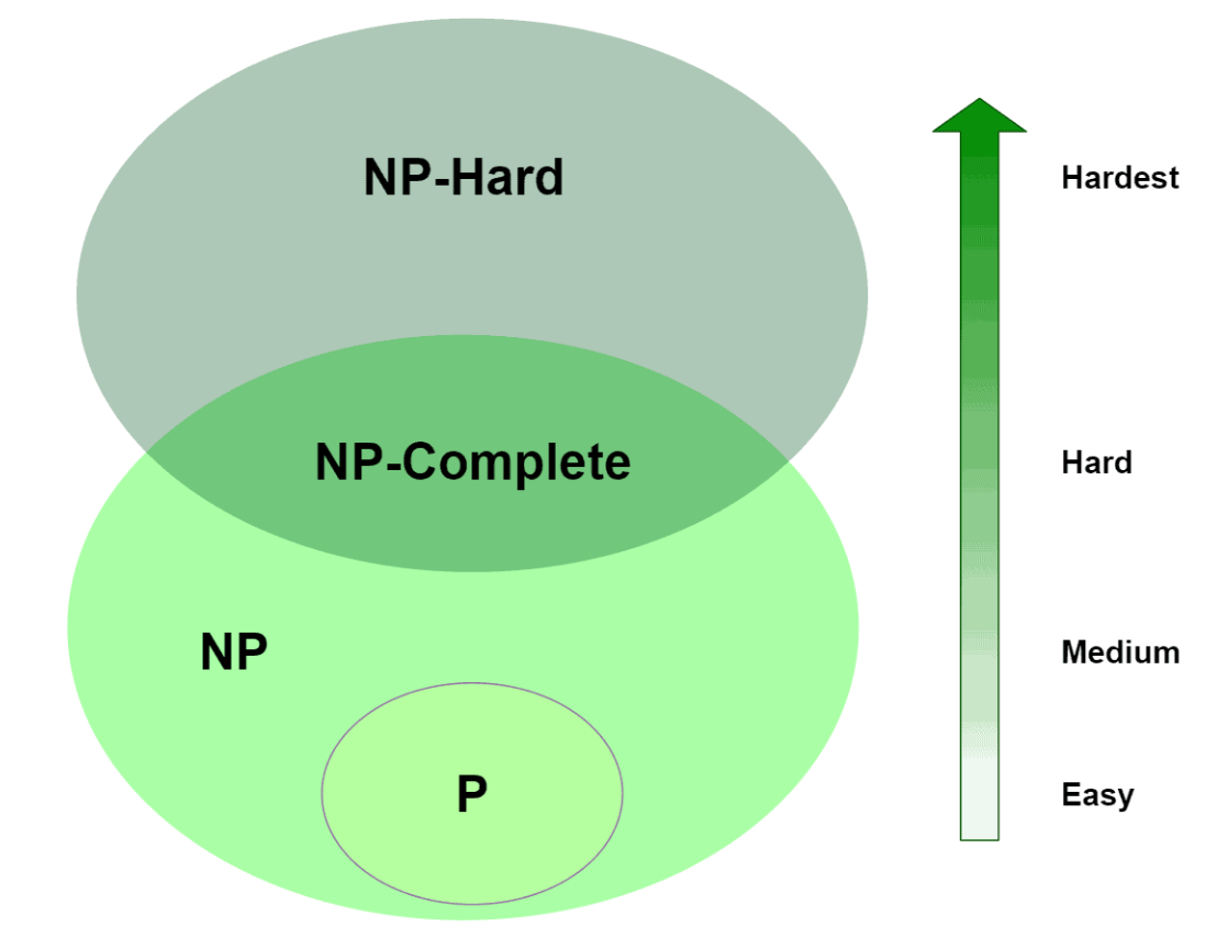
NP-Hard problems are those for which no efficient algorithm is known that can solve them in polynomial time. This means that as the problem size increases, the computational time required to solve it grows exponentially, making it practically intractable.
The significance of NP-hard problems in VLSI CAD is as follows:
- Difficulty of Optimization: Chip design is a complex problem that requires simultaneous optimization of multiple objectives such as area, performance, and power consumption. These optimization problems often exhibit NP-Hard characteristics. For example, the Placement and Routing problems in chip design are known to be NP-hard.
- Reliance on Heuristic Algorithms: Due to the nature of NP-Hard problems, EDA tools heavily rely on heuristic algorithms to find 'good' solutions within a 'reasonable' time, rather than guaranteeing optimal solutions. These heuristics must strike a balance between speed and accuracy, and sometimes may yield suboptimal solutions.
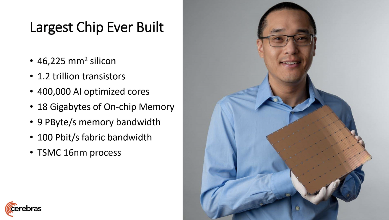
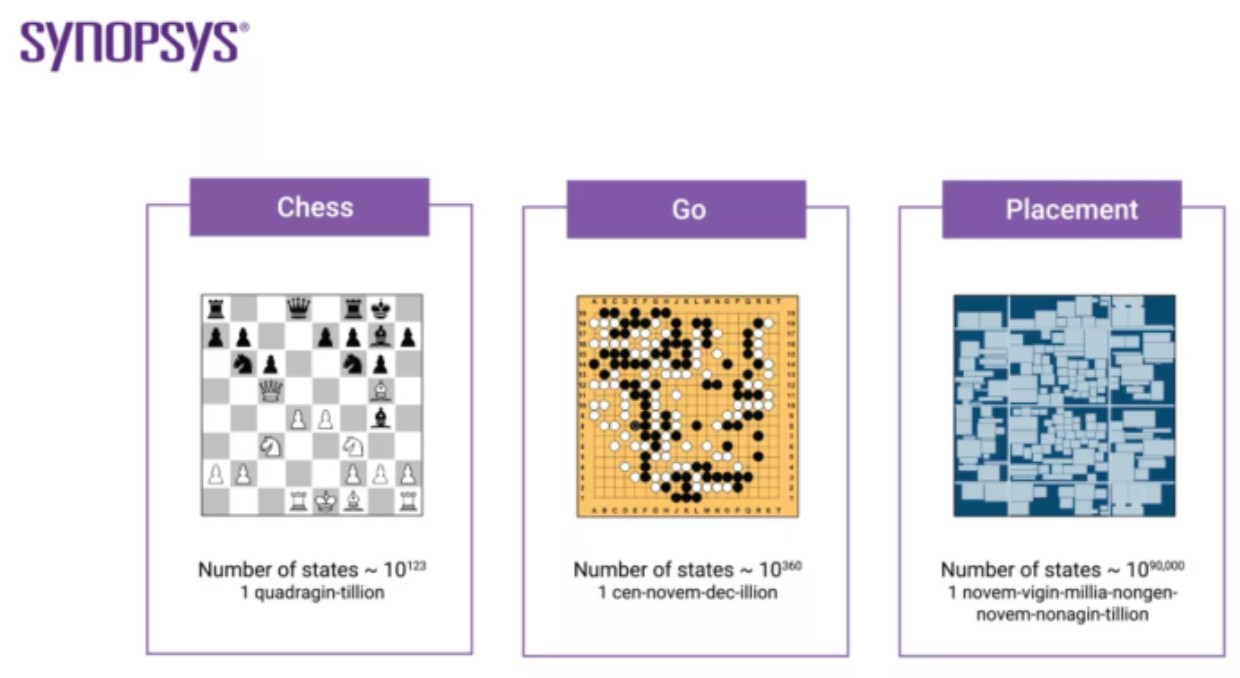
- Vast Design Space: Modern chips contain billions of transistors 1, so the number of possible design combinations is unimaginably vast. Exploring this immense design space for optimal solutions is impossible for humans and would take an enormous amount of time and cost without efficient algorithms.
Examples of NP-Hard problems in VLSI CAD include:
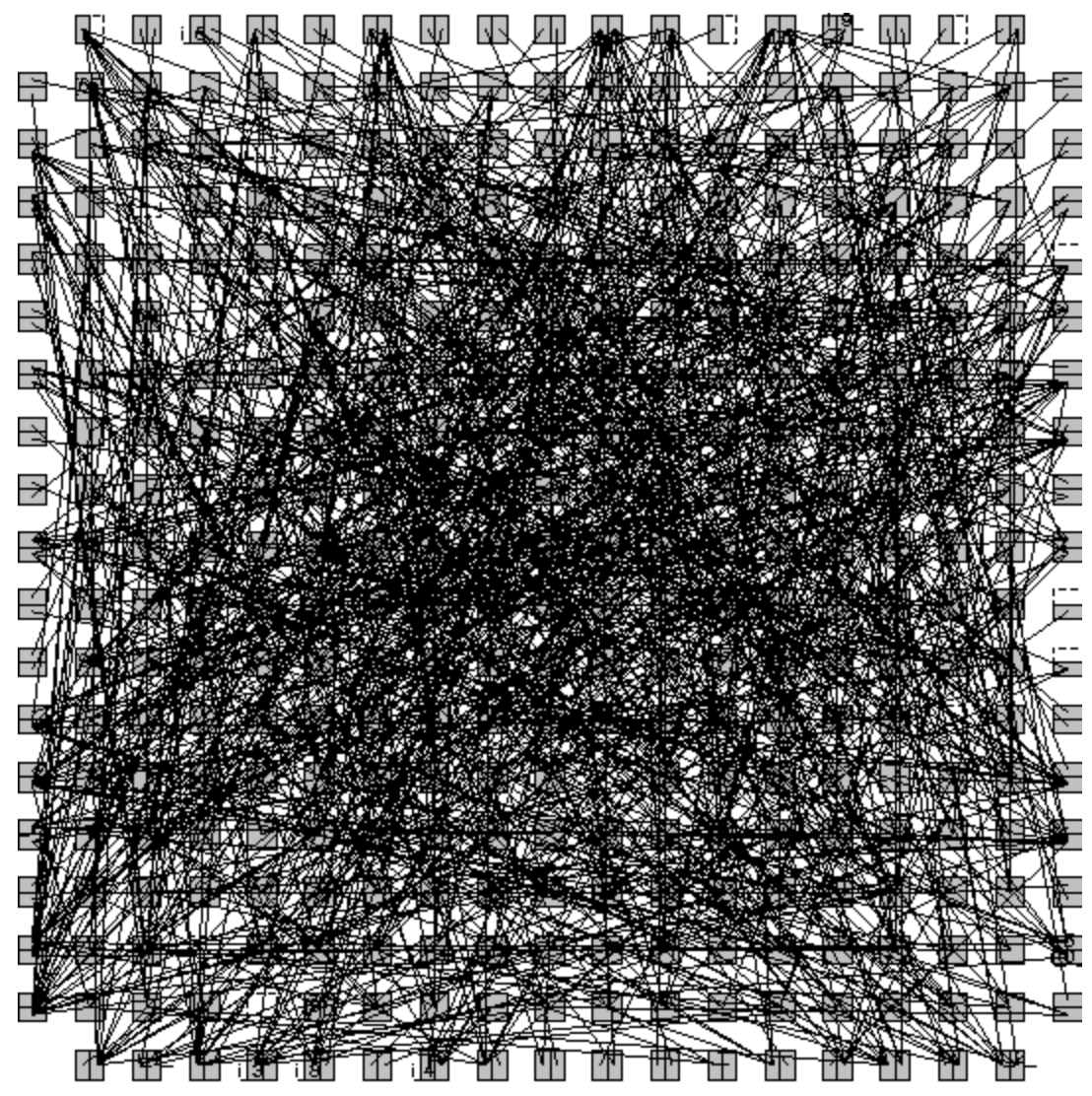
- Placement: Optimally placing millions of logic gates on a chip, considering wire length, power consumption, and timing, is an NP-hard problem.
- Routing: Connecting placed gates with wiring paths that adhere to design rules while satisfying shortest path and minimum crosstalk requirements is considered an NP-Hard or NP-Complete problem.
Despite these challenges, EDA has continuously expanded the limits of VLSI design through ongoing algorithmic improvements and advancements in computing power.
The Future of VLSI CAD: AI
Artificial Neural Network and AI are being introduced into the chip design and verification flow, opening new horizons for Power, Performance, and Area (PPA) optimization. Do you remember AlphaGo?
AI-powered EDA presents a new paradigm for design optimization that transcends human limitations, expanding the growth boundaries of the semiconductor industry.
Traditional EDA tools are often heuristic-based and may yield suboptimal solutions by trading off speed for accuracy.
Please read the article below regarding AI EDA!


The Spread of Open-Source EDA: Democratizing Chip Design
Open-source EDA tools are increasing accessibility to integrated circuit design, thereby fostering research and development.
Collaborations like Google and SkyWater Technology have led to the release of open-source process technologies such as SKY130 and SKY90-FD, offering developers opportunities to fabricate actual chips through free manufacturing shuttle programs.
OpenROAD Project: The OpenROAD Initiative is a non-profit organization supporting open-source EDA tools and innovation in the semiconductor industry.
The project's goal is to transform the traditional RTL-to-GDSII design flow into a streamlined, open-source solution.
OpenROAD also supports education and workforce development programs, helping students access chip design without the burden of license costs and complex usage models.

Conclusion: The Future Drawn by VLSI CAD
VLSI CAD and EDA are more than just a collection of software tools; they are the heart of the modern semiconductor industry and the key enablers of innovation. These technologies play an essential role in designing complex chips with billions of transistors, minimizing errors, accelerating time-to-market, and ensuring product reliability.

![[STA] Synchronous Clocks vs. Asynchronous Clocks](https://images.unsplash.com/photo-1533749047139-189de3cf06d3?crop=entropy&cs=tinysrgb&fit=max&fm=jpg&ixid=M3wxMTc3M3wwfDF8c2VhcmNofDF8fGNsb2NrfGVufDB8fHx8MTc1NTQzMzg1OHww&ixlib=rb-4.1.0&q=80&w=600)

