Why is Interconnect Delay Still Large with Advanced Process Nodes?


The continuous scaling of semiconductor process nodes improves transistor density, but it disproportionately amplifies interconnect parasitics, necessitating a "shift-left" approach where the interconnect effect, particularly resistance, must be considered much earlier and more stringently throughout the design flow.
The transition to advanced process nodes signifies a shift from a device-centric design paradigm to an interconnect-centric one. This means the importance of routing and wire delay calculation has increased. The resistance value is essential for calculating wire delay. However, due to many physical effects beyond wire delay, it is crucial to model this value accurately.
The concept of "Interconnect Integrity" in VLSI
Interconnect integrity encompasses both signal integrity and power integrity. This means a designer cannot optimize one without considering the other, as both are fundamentally influenced by parasitic resistance.
Resistance affects both signal propagation (delay, distortion) and power delivery (voltage stability, power loss). This requires resistance extraction tools and methodologies to provide an integrated view or be tightly integrated to enable comprehensive analysis of SI and PI.
The importance of accurate Resistance Extraction
As a fundamental parasitic element, resistance directly affects IR Drop across the interconnect, attenuates signal strength, and increases power consumption through Joule heating.
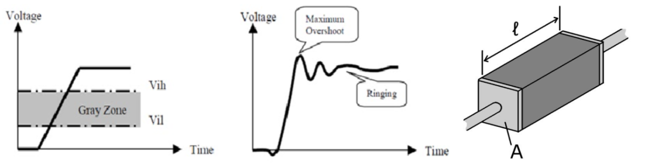
- Signal Integrity (SI): A crucial measure of electrical signal quality, ensuring reliable transmission of information throughout the chip. It is significantly affected by the interaction of resistance, capacitance, and inductance. SI degradation can manifest as ringing, crosstalk, glitches, and ground bounce.
- Power Integrity (PI): Focuses on the fidelity of the power and ground distribution networks. Interconnect resistance is a primary cause of IR drop (voltage drop) and power loss within the Power Delivery Network (PDN).
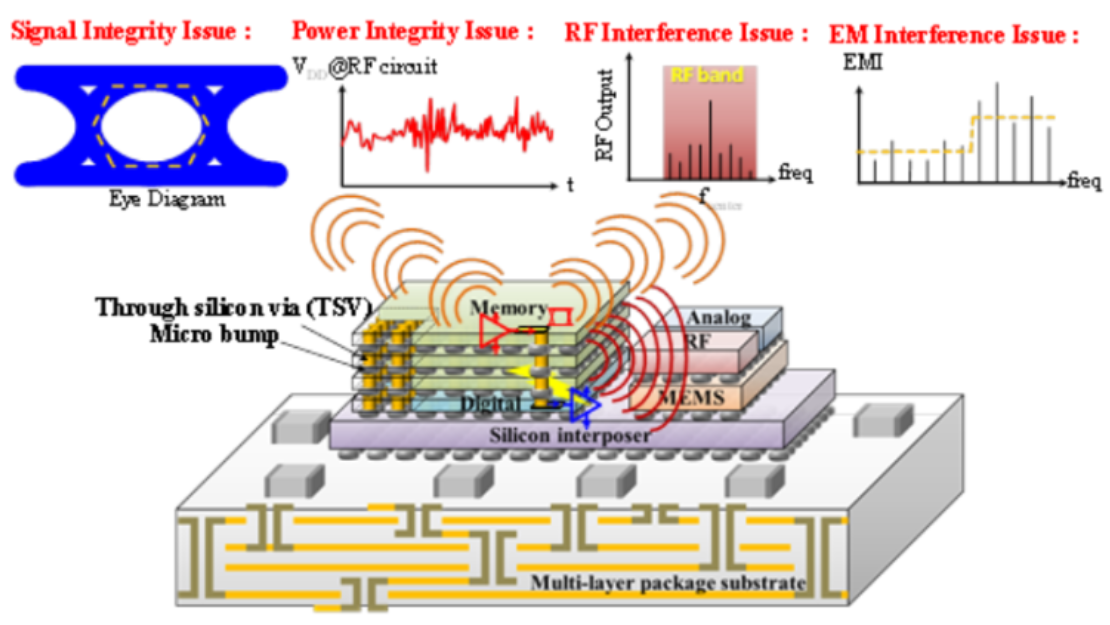

While the immediate impact of resistance on chip performance, such as signal delay, is evident, it can also affect phenomena like electromigration (EM) and IR drop. Inaccurate resistance extraction leads to incorrect predictions of current density and voltage drop, which in turn increases the risk of electromigration failures and excessive IR drop, potentially causing functional failures, reduced noise margin, and long-term chip reliability degradation.
The Impact of Process Node Scaling on Wires: Increased Resistivity, Electromigration, and Variability
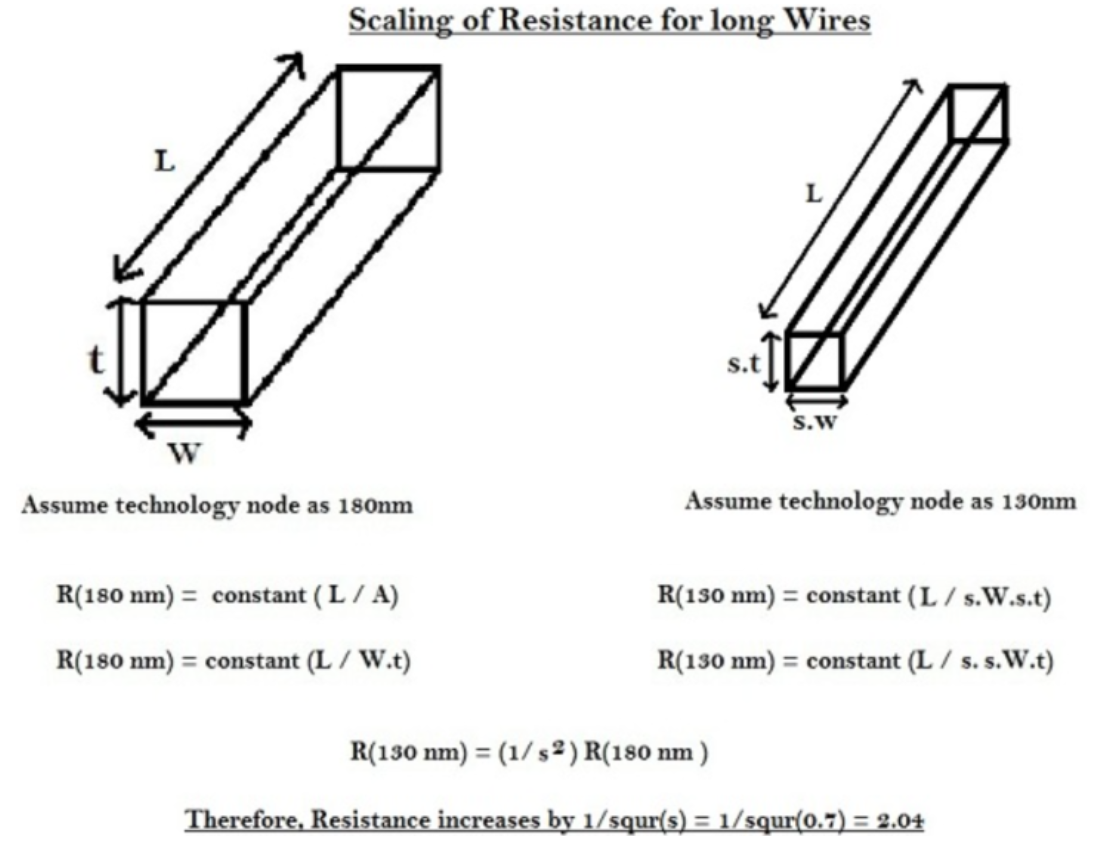
Let's assume the semiconductor process scales from 180nm to 130nm. The gate length scaling factor is approximately 0.7 (i.e., 130nm / 180nm). Therefore, s ≈ 0.7. Let's consider a short wire.
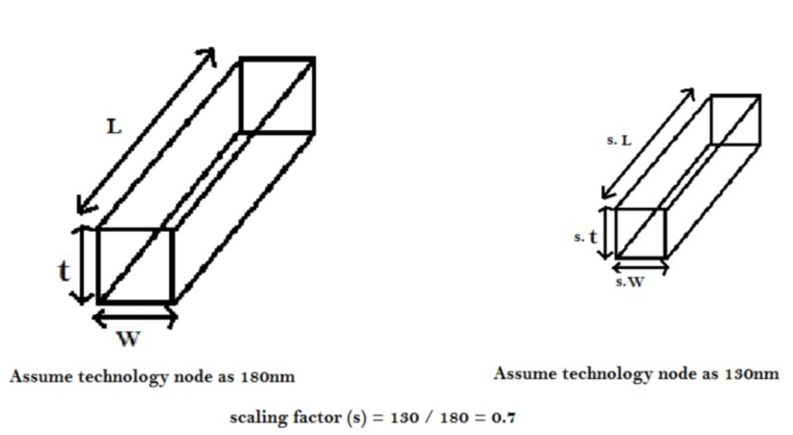
For a short wire, all three factors (length, width, thickness) scale down by the same factor, 0.7. Consequently, according to the equation below, the resistance of the short wire increases by a factor of 1.42 due to scaling.
R (130nm) = (1/s²) (180nm)
The resistivity of interconnects increases rapidly with continuous scaling, a phenomenon particularly pronounced in metal layers like M0~M1. The increase in copper interconnect resistivity at advanced nodes due to quantum mechanical scattering effects makes resistance very significant, eventually causing interconnect delay to outweigh cell delay at fine process nodes.
https://www.ansys.com/en-in/blog/what-is-electromigration
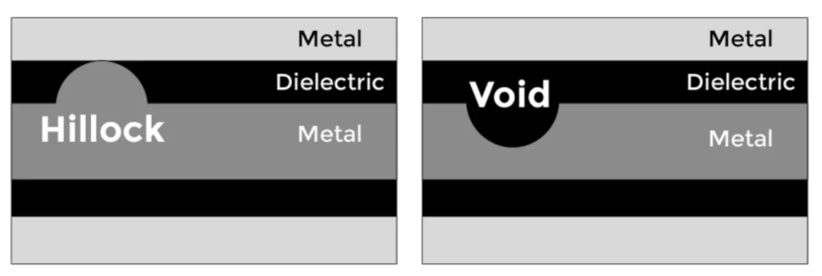
Since EM calculations also change based on the resistance value, it affects the calculation of voids and hillocks as well.
Methods for Calculating Resistance Values in Interconnects
At the most basic level, resistance extraction begins with Ohm's Law, expressed as V=IR. This law defines resistance for an ohmic material where the resistance value is considered independent of the applied voltage and current.
For a conductor with a uniform cross-section and homogeneous material resistivity, resistance can be simply calculated using the following formula:
R = ρL/A
Here, ρ is the resistivity of the material, L is the length, and A is the cross-sectional area.
However, this simple analytical formula is only accurate for very basic and ideal structures.
The wire shown above is a very smooth cylinder.
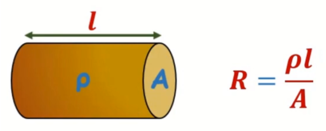
Actual metals in a semiconductor are not smooth, they are not perfect cylinders, and they are not straight lines but rather winding shapes.
As the interconnect geometry becomes more complex, incorporating bends, contacts, varying cross-sections, and intricate 3D structures, the basic assumptions of uniform current density and electric fields break down.
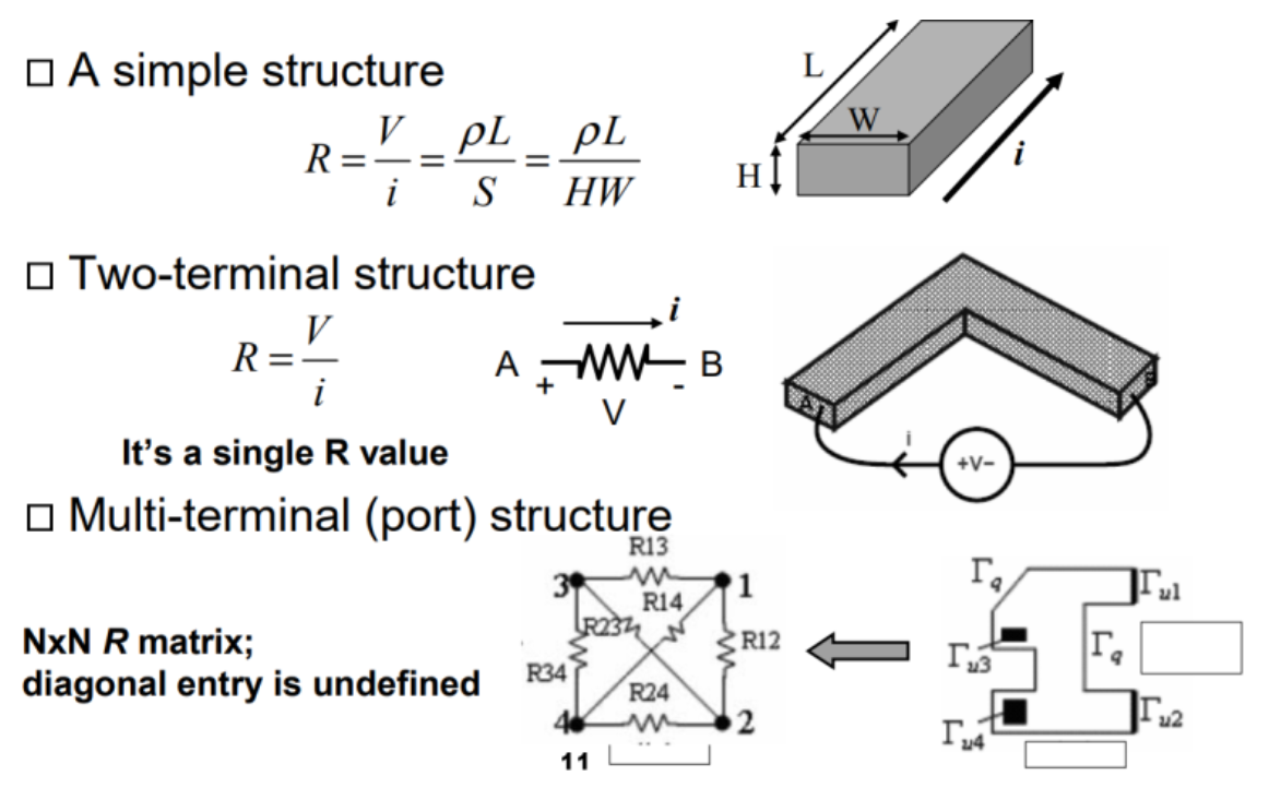
For complex interconnect structures involving multiple ports, a single scalar resistance value is fundamentally insufficient to accurately characterize the complex electrical behavior. Instead, multi-port network theory using impedance matrices (Z-parameters) or admittance matrices (Y-parameters) is used.

![[STA] Synchronous Clocks vs. Asynchronous Clocks](https://images.unsplash.com/photo-1533749047139-189de3cf06d3?crop=entropy&cs=tinysrgb&fit=max&fm=jpg&ixid=M3wxMTc3M3wwfDF8c2VhcmNofDF8fGNsb2NrfGVufDB8fHx8MTc1NTQzMzg1OHww&ixlib=rb-4.1.0&q=80&w=600)

