Yield, Harvesting Models, and the Foundry Business


Introduction
Engineering, unlike pure science, incorporates an additional crucial variable: profitability. The decision to mass-produce semiconductors hinges entirely on whether it can be done profitably.
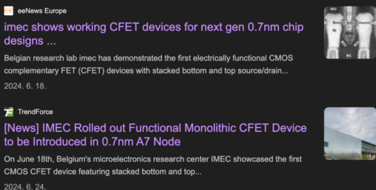
As of 2024/2025, how far have semiconductor manufacturing processes advanced? Are we at 3nm, 2nm, or 1.8nm? We have reached 0.7nm. IMEC in Belgium has already demonstrated the operation of a 0.7nm process semiconductor based on CFET technology.
So, why are 3nm process semiconductors still predominantly used in smartphones?
When introducing a new semiconductor process into mass production, the most critical consideration is "profitability relative to production cost." Semiconductor manufacturing processes demand immense investment in both initial research & development (R&D) and production facilities. Therefore, assessing the potential for profit generation is paramount for successful mass production.
The Importance of Yield
A key metric in chip manufacturing is "how many chips on a wafer are functional," which is captured by the yield. Consequently, the following engineering technologies are actively researched:
- Miniaturization of Semiconductor Process Design: Techniques to reduce the physical size of process designs.
- Accurate Modeling of Semiconductor Processes: Technologies to create models that closely resemble actual semiconductors during process design.
- Compact Chip Design: Technologies for designing smaller chips (historically preferred, but recent demands for parallel neural network processing have lowered its priority due to performance trade-offs).
- Comprehensive External Factor Verification: Techniques to recognize and verify various external factors influencing the chip.
- Circuit Design Compensation for Silicon Modeling Deficiencies: Methods to compensate for limitations in silicon modeling at the circuit design level.
- Defect Tolerance: Technologies that allow the chip to function even if some parts are defective.
- Physical Property Emulation: Technologies that accurately describe the physical characteristics of actual semiconductors.
- (We plan to delve into each of these elements in subsequent posts.)
While the Return on Investment (ROI) varies depending on R&D and production equipment investment, as well as external subsidies, the generally accepted mass production yield for leading-edge processes is "55-60%," with mature processes typically targeting "85% or higher."
Consider "Samlip Cream Bread," an ancient and popular bread in Korea, known as the nation's first mass-produced cream bread.

Just as bread production has a "process yield," operational efficiency has undoubtedly increased over time. But has the price of bread continuously fallen? No, bread prices have consistently risen, with competitors also raising their prices.
Consumers buy it if it fills them up and provides the energy they need for work. While Samlip Cream Bread's popularity might wane due to its plain taste compared to other options, it still maintains a steady customer base.
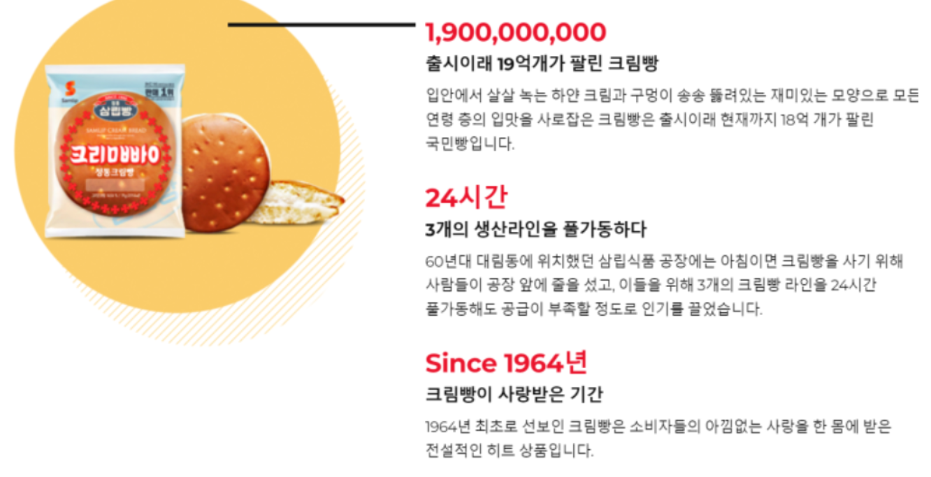
The foundry business operates similarly. Prices tend to trend upwards. If a process can create valuable products, customers will remain or new ones will emerge, even if it's an older process.
Profitability: Leading-Edge vs Legacy Processes
Leading-edge processes (e.g., 3nm, 4nm, 5nm) and mature processes (legacy processes, e.g., 45nm, 90nm, 130nm) each have advantages and disadvantages in terms of profitability, depending on their market and production stage.
High Profit Potential (Leading-Edge): Leading-edge processes like 3nm or 2nm are utilized in high-performance applications such as AI, HPC, and AP chips.
Wafers produced with these processes command premium prices, allowing TSMC and Samsung to generate substantial profits through the premium associated with cutting-edge chips. Intel, for example, is preparing for mass production of 1.8nm process semiconductors using EUV equipment.
Is the advanced process highly profitable? Absolutely!
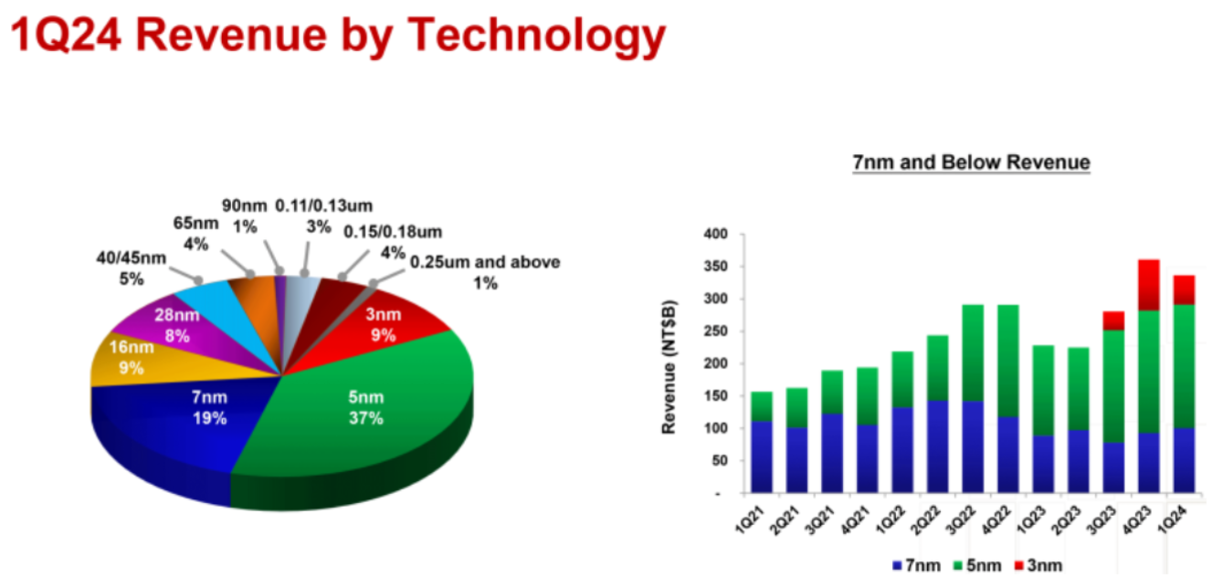
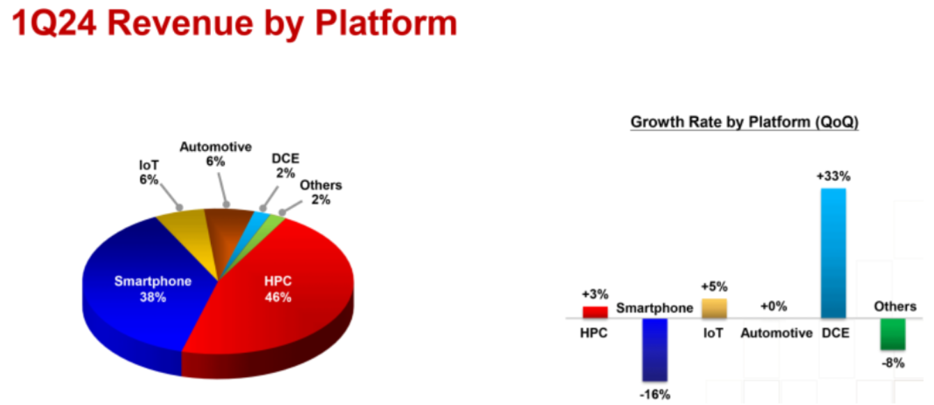
[TSMC 1Q24 Financials]
Lower Initial Yields and Profitability (Leading-Edge): Initial yields for leading-edge processes are typically low. The foundry business model is structured such that profit margins increase only when a large number of chips on a wafer are functional. This involves a continuous cycle:
(1) Receiving process orders.
(2) Observing defective chips from new masks.
(3) Analyzing discrepancies between process design models and actual silicon.
(4) Using these values to refine the next modeling iteration, and adjusting DRC (Design Rule Check) and DFM (Design for Manufacturability).
(5) Tuning process equipment parameters. This business is fundamentally about continuously improving yield.

TSMC, with its long history, naturally possesses extensive modeling history and numerous chip success stories. Its high volume of product orders allows it to execute steps (1) through (5) more frequently.
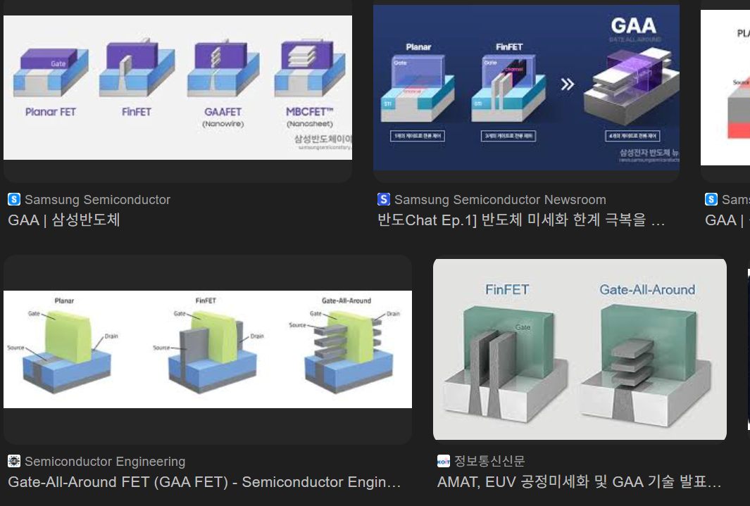
While both TSMC and Samsung use the same EDA tools and semiconductor equipment from the same companies, differences in transistor-level structures lead to yield variations.
Samsung was an early adopter of GAA (Gate-All-Around) technology for 3nm mass production, while TSMC will introduce it at 2nm. The competition in the 2nm and Sub-2nm process will be interesting to watch.
Intel's aliens seem to have moved to TSMC, so when will it be Samsung's turn?
In summary, "if a foundry receives a large volume and variety of semiconductor orders," even minor initial modeling issues can be corrected more frequently through silicon-to-model calibration during the mass production phase. In the foundry business, where yield improvement is critical, securing large orders provides a significant advantage.
Higher yield attracts more fabless customers, and higher yield boosts foundry profit margins. Crucially, receiving a large volume of mass production orders provides more opportunities to continuously refine yield, thereby enhancing price competitiveness.
- The correlation between silicon and SPICE (Simulation Program with Integrated Circuit Emphasis) modeling must be very high.
- The correlation between SPICE and the Design Kit must also be very high. Simply designing circuits with large setup/hold time margins will not yield a positive ROI for advanced process semiconductors.
- The cost of advanced equipment like EUV (Extreme Ultraviolet) lithography further reduces initial profitability. Developing leading-edge processes also requires significantly higher internal R&D investment, in addition to substantial costs for semiconductor equipment companies and EDA vendors.
- Fabless companies do not design every single semiconductor component. They focus on core designs. For example, generic designs like PCIe, USB, and Ethernet are provided by IP (Intellectual Property) vendors. These IPs must be silicon-proven and hardened. Even for USB alone, there are numerous specifications. Some foundries offer fewer than three types of USB IP for a leading-edge process, while others offer dozens for the same process. Foundries need to expand their IP offerings.
- For leading-edge processes, it's not just about swapping out equipment in an existing fab; typically, an entirely new fab must be constructed. Semiconductor equipment has different environmental specifications for manufacturing.
Some foundries bypass these steps and rely on government subsidies to continue mass production, as seen in China. Most foundries worldwide introduced ASML's EUV equipment for processes below 14nm to improve yield. However, China, facing export restrictions from the US, must use DUV (Deep Ultraviolet) equipment.
In such cases, despite immediate profitability challenges, there remains a possibility of continuously improving mass production yield through process and design technology enhancements.
Long-Term Profitability: Correlation Between Net Profit Per Chip and Process Yield
Advanced Processes:

While chip productivity is lower compared to mature processes, leading-edge processes can achieve stable yields that allow for profitable mass production.
Advanced processes become highly profitable in markets demanding high performance. In performance-driven markets like AI and consumer electronics, the high manufacturing costs of these processes can be offset by premium pricing.
Consequently, the profitability of leading-edge processes can be sustained. Over time, as production stabilizes and yields improve, the long-term profitability of leading-edge processes gradually increases. Once yields are optimized, companies can recoup their initial investment costs.
Mature Processes (Legacy Processes):
Yields reach over 90%, resulting in very high chip productivity. Processes like 28nm and 40nm have been optimized over a long period, establishing highly stable production lines.
The equipment used in these processes has often been fully depreciated, making the cost of purchasing used or new additional equipment relatively low. Mature processes are suitable for more cost-sensitive applications such as IoT, displays, home appliances, and certain automotive semiconductors (though autonomous driving and infotainment systems primarily use advanced processes).
Low production costs and high yields ensure stable profitability even with lower chip prices. While they offer high yields, the per-chip price is relatively lower compared to leading-edge processes. Mature processes are better suited for stable, cost-efficient, and high-volume production businesses.
Therefore,
(1) Higher yield attracts fabless companies to choose a foundry.
(2) Higher yield leads to higher foundry profit margins.
(3) A high volume of foundry orders provides more opportunities to conduct experiments that align design models with actual silicon characteristics.
What is a Harvesting Model?
In semiconductor manufacturing, yield refers to the percentage of chips (or dies) that function correctly after the manufacturing process and testing phase. Among various methods for predicting and optimizing yield, harvesting models are widely used.
Yield is categorized in several ways depending on the measurement target. It's important to remember that some wafers or LOT numbers exhibit better yields than others.

- Wafer Yield (Y_W): The proportion of wafers that pass testing.
- Die Yield (Y_D): The proportion of dies on a wafer that function correctly.
- Chip Yield (Y_C): The proportion of individual chips that pass testing after packaging.
In the simplest case, yield is calculated as follows: [Image: Simple Yield Calculation Formula - please insert appropriate formula here, e.g., (Number of Good Dies / Total Number of Dies) * 100%]
However, in reality, it is far more complex. Defects occurring during the manufacturing process can be influenced by die size or technology node.
Types of harvesting models include Poisson and Binomial Models, Murphy, Seeds, and Bose-Einstein Models. The most commonly used are the Poisson model and the Murphy model.
What is the Poisson Model in Semiconductor Yield?
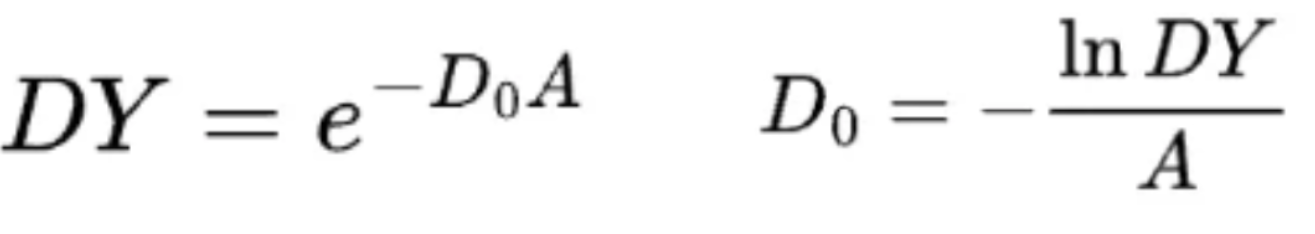
Assuming D0 is the defect density per square centimeter and A is the die area in square centimeters, then λ0 = D0 × A. For a die to be functional, the number of defects must be zero. Therefore, the die yield (DY) is P(k=0) and is modeled by a simple exponential function:
[Image: Poisson Model Formula - please insert appropriate formula here, e.g., DY = e^(-λ0)]
For a 1 square centimeter chip: Assuming D0 = 0.4/cm², the die yield is 67%. Assuming D0 = 0.1/cm², the die yield is 90%.
Reference:https://www.viksnewsletter.com/p/how-foundries-calculate-die-yield
Factors Affecting Yield
Key factors influencing yield loss include:
- Defects Per Unit Area (DPU): Defects can arise from contamination, design flaws, equipment issues, etc.
- Die Area (A_D): Larger die sizes generally increase the probability of defects.
- Process Maturity: Cutting-edge processes may have lower initial yields compared to mature processes.
- Design Complexity: Complex designs can increase the likelihood of defects.
For reference, the market is predicting the price range for the soon-to-be-released Qualcomm Snapdragon 8 Gen 4 to be $200-240 USD, and MediaTek Dimensity at $150-200 USD.https://biz.chosun.com/it-science/ict/2024/10/04/ZS62NOTASBBFDCOFZV5SP6DVFE/?outputType=amp
Conclusion
Short-Term Profitability: Advanced processes offer efficient PPA (Performance, Power, Area), making them suitable for cutting-edge applications requiring low power and high performance. Due to lower initial yields and higher costs, they command a premium, resulting in a high price per chip. Profitability increases as yield stabilizes.
Long-Term Profitability: While leading-edge processes may have low initial profitability, they can expect greater long-term profitability as yields improve and market demand for high-performance chips persists.
To achieve high yields, process accuracy is crucial, and extensive orders are necessary to gain experience and ensure that design modeling values align with actual semiconductor characteristics. The Poisson model and Murphy model are frequently used for yield calculation.
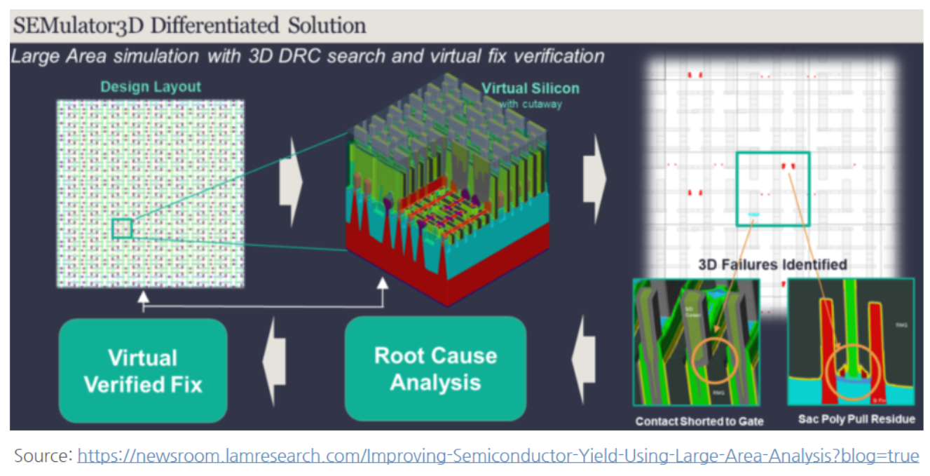
I highly recommend watching the following video to understand the "comprehensive solution for yield improvement" envisioned by EDA companies. [Please insert a valid YouTube URL here, as the provided URL was a placeholder.]
References:
- https://images.samsung.com/is/content/samsung/assets/global/ir/docs/2024_2Q_conference_eng.pdf
- https://www.anandtech.com/show/21359/tsmc-posts-q124-results-3nm-revenue-share-drops-steeply-but-hpc-share-rises
- https://www.mckinsey.com/industries/semiconductors/our-insights/whats-next-for-semiconductor-profits-and-value-creation
- https://www.bcg.com/publications/2023/navigating-the-semiconductor-manufacturing-costs
Many of you likely know more about the foundry business than I do. I've written this article to open a dialogue. I'd love to see your "Insider's View" in the comments! I'm sure some of you thought, "Wait, that's not quite right!" while reading this—please, correct me! That's precisely why I wrote this, despite it being a field I'm still learning about and despite my embarrassment, so I can learn from you all!


![[STA] Synchronous Clocks vs. Asynchronous Clocks](https://images.unsplash.com/photo-1533749047139-189de3cf06d3?crop=entropy&cs=tinysrgb&fit=max&fm=jpg&ixid=M3wxMTc3M3wwfDF8c2VhcmNofDF8fGNsb2NrfGVufDB8fHx8MTc1NTQzMzg1OHww&ixlib=rb-4.1.0&q=80&w=600)

